Download
1 / 28
300 likes | 507 Views
A 77-79GHz Doppler Radar Transceiver in Silicon. Sean T. Nicolson 1 , Pascal Chevalier 2 , Alain Chantre 2 , Bernard Sautreuil 2 , & Sorin P. Voinigescu 1

E N D
A 77-79GHz Doppler Radar Transceiver in Silicon Sean T. Nicolson1, Pascal Chevalier2, Alain Chantre2,Bernard Sautreuil2, & Sorin P. Voinigescu1 1) Edward S. Rogers, Sr. Dept. of Electrical & Comp. Eng., University of Toronto, Toronto, ON M5S 3G4, Canada 2) STMicroelectronics, 850 rue Jean Monnet, F-38926Crolles, France
Outline • Motivation and applications of Doppler radar • Transceiver architecture and implementation challenges • Circuit design and layout (top level & circuits blocks) • Fabrication technology and measurement results • Detection of the Doppler shift
Doppler Radar Review • Track range and velocity of a target without amplitude info • Target range: • Target velocity: transmitted carrier (fC) Doppler shift hostile channel fC ± Df moving target (v) transceiver reflected signal round trip delay (t)
Automotive Radar Applications • Automotive applications of Doppler radar • Transceiver requirements: • Long range, high PTX (not CMOS) • On-chip DSP (need CMOS) • low cost, single chip (many per car) • Low area, low power (phased arrays) • SiGeBiCMOS, direct conversion < 1 part/billion sensitivity c = 3×10⁸ v = 1 km/h fC = 77GHz 150-200m Dv < 1km/h Df = 70Hz
Implementation of the Transceiver • Single die for receiver and transmitter • Tuned clock tree used to distribute VCO signal • Frequency division at 77GHz using a static divider • All circuit blocks use < 2.5V supply (except divider uses 3.3V)
Implementation of the Transceiver Complete power and bias isolation VCO supply LNA supply Digital supply • Single die for receiver and transmitter • Tuned clock tree used to distribute VCO signal • Frequency division at 77GHz using a static divider • All circuit blocks use < 2.5V supply (except divider uses 3.3V)
Low-noise Amplifier 250mm • 3-stage design, add R1 to de-Q the final stage. • Noise & Z matching inc. CPAD [Nicolson et al., CSICS 2006] • All circuit blocks discussed in [Nicolson et al., IMS 2007] 1pF decoupling caps
Clock Buffer Design • Cascode topology is chosen for the clock buffer • high reverse isolation (i.e. low S12) • Broadband, low gain (degeneration and resistive loading) • Parameterized design of fixed size buffer to variable size load • Q1, Q2, LC, and LE are fixed • R1/R2 chosen for biasing, R1//R2 chosen to set Q • LINT and C1 chosen to match to particular HBT size matching interface
Layout for Isolation & Bias Distribution • Layout methodology systematically addresses: • Isolation of circuit blocks • High-C, low-R, low-L power, ground & bias planes • N-well and p-sub contacts for isolation in the substrate
Top Level Layout 0.9mm 1.3mm
Fabrication Technology Technology info in: [P. Chevalier et al., BCTM 2005] • Two technologies with identical BEOL • wE = 0.13mm with 170/200 GHz fT/fMAX • wE = 0.13mm with 230/290 GHz fT/fMAX
Transmitter Output Power • Transmitter POUT vs. LO and T (230/300GHz fT/fMAX process)
Optimal Biasing for SiGe HBT PAs • SiGe HBT power amplifier PAE, PSAT, and P1dB vs. bias • All reach a maximum at the same current density 1.8V 1.5V
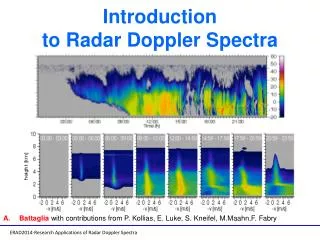
Receiver Conversion Gain • Peak conversion gain of 40dB, -3dB bandwidth is 10GHz 83GHz LO Conversion Gain [dB] 78GHz LO 81GHz LO
Receiver Conversion Gain • IP1dB of -35dBm and OP1dB of +3dBm at 25°C, 2.5V supply • IP1dB of -30dBm and OP1dB of 0dBm at 100°C, 2.5V supply 83GHz LO
LNA Input Match • S11 better than -15dB from 81GHz to 94GHz • S11 does not degrade significantly with current density
Receiver Noise Figure @ 1GHz IF • JOPT is constant versus temperature bias with const. IC • 3.85dB NF at 25°C in receiver with 300GHz fMAX HBT 81.6GHz LO 3.85 dB
Receiver Noise Figure versus IF • Maximum NF of 4.7dB at 2.5GHz IF, 81.6GHz LO 4.7 dB
Doppler Radar Experimental Setup IA ACL = 40dB Bias 30Hz DC block 3kHzLo-Pass BNC cables Scope 110GHz probe & cap 110GHz probe & cap 15cm 110GHzcoax 4dB RX loss Target 0.25m26m range 12dB TX loss 107dB channel loss > 40cm 110GHz coax horn antennae(20dB gain each)
Doppler Radar Experimental Setup > 40cm of 110GHz coaxial cable
Example Doppler Signal • 55Hz Doppler signal (target moving at 0.75km/h)
Doppler Radar Video • Human target walking forward & backward at varying speed
Comparison To Other Work • This work: bottom row
Conclusions • First single-chip silicon 82GHz direct conversion transceiver • Fundamental VCO • Verified to operate at 100°C using 2.5V supply (3.3V for divider) • Improved VCO will obtain improved performance over temperature • Static frequency divider at 82GHz • Successfully detected a 55Hz Doppler shift at 6m range • 3.9 – 4.7dB noise figure with 82GHz LO and 0.5 – 4GHz IF • record for W-Band CMOS/SiGe receivers
Acknowledgements • K. Yau for help with measurements • STMicroelectronics for fabrication of circuits & test structures • J. Pristupa, and E. Distefano for CAD & network support • CITO & NSERC for funding