Download
1 / 15
150 likes | 200 Views
This outline provides a work plan and proposal for the MISTRAL-in circuit, specifically focusing on a sensor variant for larger radii. The proposal includes details on the running conditions, double-sided readout (DSR) and single-sided readout (SSR) options, power consumption, and digital development requirements. The work plan outlines the testing and evaluation of different chip designs and technologies, as well as the integration of pixel arrays and discriminators.

E N D
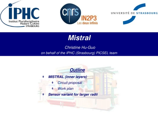
MistralChristine Hu-Guoon behalf of the IPHC (Strasbourg) PICSEL team Outline • MISTRAL (inner layers) • Circuit proposal • Work plan • Sensor variant for larger radii
MISTRAL-in (Inner layers) • Running conditions: • 30-35 °C, 2 MRad, 2x10^13 Neq/cm² • Proposal: active area: ~10 x 30 mm² • Double Sided Readout (DSR) • Power consumption: ~1200 mW/sensor • ~400 (~250) mW/cm² • Single Sided Readout (SSR) • Power consumption: ~600 mW/sensor • ~200 (~160) mW/cm² 1 common digital development for both versions, only doubled for DSR IPHC christine.hu@ires.in2p3.fr
~1 cm ~1 cm 512x256 512x256 512x256 Discriminators Discriminators Discriminators SUZE SUZE SUZE MUX MUX MUX Memory 1 Memory 1 Memory 1 Memory 2 Memory 2 Memory 2 MISTRAL-in (e.g. Single-Sided Readout SSR) • Proposal for a modulo design: • Overcome design complexity (frequency, readout time, layout) over 3 cm long sensor • Reuse the basic block for other applications • Easy for prototype evaluation, the basic block should incorporate all pads needed for tests Independent blocks Serial read out IPHC christine.hu@ires.in2p3.fr
SUZE-02 • Based on MIMOSA26 and ULTIMATE design principle • Occupancy 5.2 x10^5 hits/cm²/s (Costanza, 20 June 2011) • Parallel search in 8 banks (64 columns/bank) • No. of states per bank • Combine the outputs of the 8 banks • No. of states per raw • Safety factor x 4 • Safety factor x 5 Assume each hit activates 3 contiguous rows State: Up to 4 contiguous pixels with output above threshold • Readout time 200 ns/row (based on 0.35 µm process, perhaps shorter in 0.18 µm) • Fraction of noisy pixels 10^(-4) • Overflows per bank & per raw < 0.1% • Calculation for worst case, 2 memories in pipeline mode, 16 bits / word IPHC christine.hu@ires.in2p3.fr
SUZE-02 • Accounting for the effect of long term irradiation (Noise , Signal ): • 6 states per bank • 12 states (or more, up to 16? 4-bit encoding) per group of 512 columns • Memory: 16-bit/word not yet optimised • Silicon surface & data flow • Output bit rate for whole, 3 cm long, sensor : ~ 800 Mbits/s (safety factor = 5, SSR, memory: 16-bit/word) • In case of fake rate ~10^(-3), foresee ~1Gbit/s • In case of single output (SSR), a digital modulation seems mandatory • Within 1 clock cycle, more than 1 bit can be sent IPHC christine.hu@ires.in2p3.fr
Work Plan: MISTRAL-in (1) • RAMSES (INMAPS 0.18 µm) tested in April/May 2011 at IPHC • ENC~20-50 e-, wide noise dispersion, • Contact with designer, investigation on going • MIMOSA30 (0.35 µm) design on going, submission: Sept. 2011 • Evaluate elongated pixel (16x64 µm²) and readout from both sides • MIMOSA32 1st prototype in Tower CIS 0.18 µm technology • Motivation for CIS 0.18 µm: • Small technology feature allows: • Radiation tolerance , • Read-out speed , • Power consumption , • Si surface (periphery) • 6 metal levels may suppress dead zone (steering logic control part) • Optimised sensing systems available and tunable enhanced SNR • High-resistivity epitaxy (1 - 5 kΩ · cm) enhanced SNR • … • Deep P well PMOS transistors permitted (radiation tolerance detection efficiency?) • Improve pixel performance, integration of intelligence within pixel IPHC christine.hu@ires.in2p3.fr
STAR collaboration Work Plan: MISTRAL-in (2) • MIMOSA32 submission: end of Oct. 2011: Chip dimension: ~3x8 mm² • Technology exploration & evaluation • Sensing device optimisation • Pixel optimisation: in pixel amplifier (PMOS?) • Basic pixel size: 20x20 µm², but also 20x40 and 20x80 µm² • Develop building blocks: amplifier, column-level discriminators, LVDS, … • Evaluate digital circuit w.r.t. latch up! • SUZE, Mimosa22 and Phase-1 are more susceptible to latch up than Mimostar2. • SUZE is more susceptible to latch up by a factor of ~5. IPHC christine.hu@ires.in2p3.fr
A trial to suppress dead zone It may be done with 6 ML 128x128 Discriminators 512x256 512x256 512x256 Discriminators Discriminators Discriminators SUZE SUZE SUZE MUX MUX MUX Memory 1 Memory 1 Memory 1 Memory 2 Memory 2 Memory 2 Discriminators Work Plan: MISTRAL-in (3) • MIMOSA22THR (3 circuits?): submission June 2012 • Estimated total chip dimensions ~80 mm² • Integration of pixel array + discriminators • Both have been tested in Mimosa32 • Test the most critical sub-circuits • SEU tolerance design for critical parts • Decision:after irradiation test, make a choice • 1. Pixel 20x20 vs 20x40 µm² 2. DSR vs SSR • SUZE-02: submission June 2012 ? • Evaluate: latch-up tolerance, memory design (IP? who?) • FSBB(~ 1.3 cm²): submission Q2/2013 • Proposal: basic modulo block • MISTRAL (e.g. SSR ~4 cm²): submission Q2/2014 • Synchronisation of three blocks • Clock distribution • Serial transmission (should be studied before) 128x526 Red: (4 signals) PWR_ON, Slct_Row, Slct_Grp, Clp Green: Column line of pixels output FSBB: Full Size Building Block Serial read out IPHC christine.hu@ires.in2p3.fr
Sensor variant for larger radii • Running conditions: • 30-35 °C, less than 50 kRad (estimated), less than 5x10^11 Neq/cm² (estimated) • Active area: ~20 x 30 mm², readout: SSR • Pixel width ~ 20 µm may be an extension of MISTRAL-in • Discriminators ending each column Not adapted to dE/dx measurement • Power consumption: ~600 mW/sensor, ~200 (~160) mW/cm² May benefit from the digital development of MISTRAL • Pixel width ~ 40 µm • n (?) -bit ADC ending each column dE/dx measurement • Power consumption: ~500 (?) mW/sensor • Need new SUZE development & for n>4, need ADC development FTE • Modulo design proposal should still be valid for both designs IPHC christine.hu@ires.in2p3.fr
128 x 32 128 x 16 Discriminators Existing Prototype: MIMOSA22AHR (1) • MIMOSA22AHR (0.35 µm) submitted & tested in 2010 • EPI: ~400 Ω.cm, thickness: 10, 15, 20 µm (Standard EPI: ~10 Ω.cm, thickness: 14 µm) • 16 different sub matrices connected to discriminators • 128 columns: binary output + 8 columns: analogue output • 2 sub-arrays (2/16) featuring elongated pixels • 18.4x36.8 µm² (S15) & 18.4x73.6 µm² (S16) • Low diode density CCE • Irradiation Leakage current Noise • Globally: enhanced vulnerability to radiation S11 S15 S16 IPHC christine.hu@ires.in2p3.fr
Existing Prototype: MIMOSA22AHR (2) • Lab test @20 & 35°C, @3x10^12 Neq/cm², @150 kRad • Preliminary beam test results at SPS (T ~20°C, before irradiation): • Analogue readout: region limited statistics limited • S/N (seed) ~ 30 • Digital output: overall satisfying performances • No significant loss in detection efficiency: eff >~ 99.8% for a 10-5 fake rate • No inefficient region observed (but statistics small) • Spatial resolution satisfactory • S15 ~ 4.7 m ; S16 ~ 6 m (binary charge encoding) A. DOROKHOV IPHC christine.hu@ires.in2p3.fr
Other sensors (0.35 µm process) planned for submission • MIMOSA29: test structure for large pixels to be submitted in June 2011 • 64x16 µm², 64x32 µm², 64x64 µm² • 1, 2 or 4 diodes in a pixel • 80x16 µm², 80x48 µm², 80x80 µm² • 1, 2 or 4 diodes in a pixel • MIMOSA31 design on going, submission: Sept. 2011 • 1st sensor incorporating pixel array with ADC ending each column • Pixel: 35x35 µm² • ADC: "4" bit (4-3-2 bit) • ADC is based on a successive approximation • Architecture requires 4 cycles to complete one conversion • These sensors act as forerunners for possible R&D of sensors adapted to large radii • Translate design from 0.35 to 0.18 µm? • dE/dx measurement may require a dedicated ADC development SUZE development IPHC christine.hu@ires.in2p3.fr
Summary • A baseline CMOS pixel sensor adapted to the specifications of L0 + ... is likely to be achievable by 2014 • It is based on the ULTIMATE (MIMOSA28) chip realised for the STAR-PXL • 0.18 μm CMOS technology expected to comply with radiation tolerance specifications • DSR or SSR 40-50 or 20-25 μs readout time (NI rad. tolerance vs pitch) • Room temperature operation (air flow) • Work plan (MISTRAL-in): 4 submissions • Oct. 2011 MIMOSA32: technology exploration, pixel optimisation, building blocks, latch-up evaluation for digital part • June 2012 MIMOSA22THR: integration of pixel array + discriminators, test of most critical sub-circuits, SEU tolerance design for critical partsSUZE-02: latch-up tolerance evaluation, memory design • Q2/2013 FSBB: development of the basic modulo block • Q2/2014 MISTRAL: final sensor • MISTRAL-out: 2 possibilities: • Extension of MISTRAL-in: pixel 20x80 µm², discriminators ending each column • Alternative (R&D needed): pixel 40x80 µm², n(?)-bit ADC ending each column new SUZE IPHC christine.hu@ires.in2p3.fr
Back up IPHC christine.hu@ires.in2p3.fr