ASKAP Feeds
ASKAP Feeds. David DeBoer ASKAP Project Director 05 May 2009. ASKAP Design Goals. High-dynamic range, wide field-of-view imaging Number of dishes 36 (3-axis) Optics prime focus f/D 0.5 Dish diameter 12 m Surface < 1mm Pointing 30 Max baseline 6km


ASKAP Feeds
E N D
Presentation Transcript
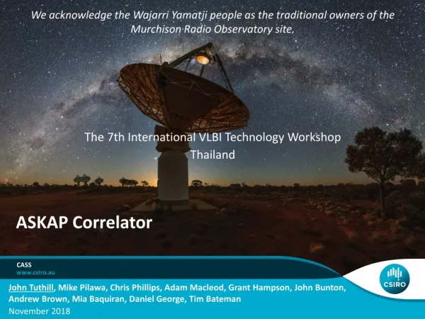
ASKAP Feeds David DeBoer ASKAP Project Director 05 May 2009
ASKAP Design Goals High-dynamic range, wide field-of-view imaging Number of dishes 36 (3-axis) Optics prime focus f/D 0.5 Dish diameter 12 m Surface < 1mm Pointing 30 Max baseline 6km Sensitivity 65 m2/K Speed 1.3x10⁵ m4/K2.deg2 Observing frequency 700 – 1800 MHz Field of View 30 deg2 Processed Bandwidth 300 MHz Channels 16k Focal Plane Phased Array 188 elements + Infrastructure for new SKA-ready observatory Murchison Radio Observatory (MRO) + Support of other projects (MWA, PAPER, +)
Receivers/Data Transport High-Z, differential low-noise amplifiers ~3:1 Up-conversion Analog fiber to BF Receiver-on-a-chip
ASKAP data flow, processing, and storage CSIRO. SKA2008
Analog Systems IPT team • Low-noise amplifier design • Rob Shaw • Peter Axtens • Receiver electronics • K. Jeganathan • Simon Mackay • Suzy Jackson • Yoon Chung • Plus consultation services of: • Pat Sykes • Michael Brothers • Matt Shields • Mark Bowen • Santy Castillo • Henry Kanoniuk • Les Reilly Russell Gough (IPT leader) John O'Sullivan (IPT scientist) • Electromagnetic design of FPA and calibration system • Stuart Hay • Rong-Yu Qiao • Francis Cooray • Doug Hayman • Aaron Chippendale • Mechanical design • Deszo Kiraly • Russ Bolton • Paul Doherty • Eliane Hakvoort • Workshop staff (3 EFT)
Introduction - Analog Systems • The ASKAP analog system • amplifies astronomical signals, frequency translates (twice) and filters the signals before they are sampled by the ADC. • The ASKAP analog system includes • the “Chequer-board” Focal Plane Array • the prime focus electronics package • the pedestal analog electronics package • calibration signalling system • The calibration signalling system • allows the complex gain of each receiver channel to be measured and monitored. • uses three dual polarisation radiators on the reflector surface. (One radiator on bore-sight the other two off-axis)
Scope of Analog Systems IPT • The “Chequer-board” Focal Plane Array • Electromagnetic design • Optimisation of Chequer-board array and low-noise amplifiers • The prime focus electronics package, which includes: • the balanced low-noise amplifiers, each with a post-amplifier gain-slope equalizer • broadband bandpass filters and switchable sub-band select filters • driver amplifiers to send the RF signals from the prime focus electronics package to the pedestal analog electronics package • control and monitor electronics and power supply filtering • The calibration signalling package.
Analog System specifications • Frequencies • RF band 700 – 1800 MHz • Instantaneous bandwidth 300 MHz • Sampled band 424 – 724 MHz • Sample clock 768 MHz • Low-noise amplifiers • Low-noise amplifier noise temperature 40 Kelvin • Low-noise amplifier gain 27 dB • Gain • Nominal total nett gain 72 dB • Nominal nett gain at prime focus 68 dB • Assumed loss in cable 17dB at 0.7 GHz (from prime focus to pedestal) 31dB at 1.8 GHz • Nominal nett gain in pedestal 21dB at 0.7 GHz 35dB at 1.8 GHz • Output power (to digitiser) • Nominal output power -19 ±1 dBm into 50 Ohms
Timeline and Milestones • March 2009: Analog Systems PDR • March 2009 - September 2009 Build and test first prototype of Analog System • September 2009: Analog Systems CDR • September 2009 - April 2010 Build and test Analog System for Antenna #1 • April 2010: Antenna 1 construction complete • April 2010 - June 2010 Install Analog System in Antenna #1 • June 2010: Complete installation of equipment in Antenna #1 • June 2010 - November 2010 Build and test Analog Systems for Antennas #2 - #6 Install Analog Systems in Antennas #2 - #6 • November 2010: Complete installation of equipment in Antennas #2 - #6
System-on-a-chip Other design options Microcooling
Digital beamformer FPA concept Patches Transmission lines • Connected checkerboard array Currents Low-noise amplification and conversion Ground plane Weighted sum of inputs
FPA Package design FPA Electronics housing RF outputs in weatherproof ports DC / Control and cooling ports RFI shield and weather proof octagonal enclosure Additional Antenna leg attachment point Rigid focal plane baseplate Main Antenna leg bracket fixture
FPA Package internal design Isolated cable interface bulkheads Centralised cooling Circulation fans on air baffle Module conduction cooling plates
Cooling conduction and air circulation Module mounting and cooling plate Cooling air upward vents Module guides and heat conduction path
LNA RF shield and heatsinks Cooling air galleries LNA assembles and RFI shield heatsinks
FPA mounting FPA dielectric weather shield Baseplate relief for conduction reduction Antenna leg mounting points
Approach to the design • Development of modelling capability • Modelling and experimental investigations of 5x4 array • Refined and enlarged design for ASKAP
Modelling capability Plane wave/ radiation pattern ports Array ports (eg at groundplane) • YA: CBFMoM, GEMS, MWS, PO • YL and LNA noise: MO, measurements on LNA, MWS transitions • Vb (signal + noise) by cascading Y and equivalent-current covariance matrices • Software checking by independent codes Array and reflector Sources and spillover Temperature T Flux density S Vbeam= wtoVo LNA+ Gmaxavailable
IL,i¯ IL,i¯ IA,i¯ IA,i¯ IL,iD IS,i¯ IS,i¯ VA,,i¯ VA,i¯ ZL,i VL,i¯ g VL,i+ IL,iC ZL,iD VL,iD ZL,iC i¯ ZL,i VA,i+ VL,i+ VA,i+ VL,iC IS,i+ 2a i+ IS,i+ IL,i+ IL,i+ VA,i¯ IA,i+ IA,i+ IA,i¯ VA,i+ IA,i+ 2b Loading/beamforming configurations Differential: Single-ended: Differential single-ended:
ηtot verses loading/beamforming configurations f/D=0.4 f/D=0.5 Differential: LNA stability and array resonance problems Single-ended: Good but not worth x2 electronics Differential single-ended:Current focus
Radiation-pattern test configuration • SE patterns easiest to test before LNA available • SE ports :50ohm SMA connectors • Differential loads: nominal 300ohm resistors
Effects of dielectric PCB (RO4003C) • Noticeable in radiation patterns • Some variation in Zopt (eg 30% increase at 1.5GHz) • Small addition to Tsys: (conductor+dielectric) < 3K
MWS vs measured radiation patterns • Adaptive meshing has also resulted in much improved agreement with measurements
Differential radiation patterns • LNA asymmetry requires general 3-port model to characterize • Patterns dependent on LNA port / array port mapping
Preliminary design of ASKAP-sized array • FoV 30 sq deg requires larger array • 11x10 minus some corner elements • 188 diff ports (112) patches
LNA Schematic ATF-35143 PHEMTs Symmetric structure
These are the generations • Version 1: the design I inherited, with slight revisions. Installed on Parkes 5x4. • Version 2: redesigned for lower input capacitance.
A sample noise temperature measurement Version 1 noise temperature
Performance (I) Version 2 noise temperature
Performance (II) Version 2 diff-mode input impedance
Performance (III) Version 2 gains
Parkes Observations • Phase 1 • Single dish, single 8 by 8 real time full correlator 0.875 MHz BW • GPS L2 (1227.6 MHz, 10 Mchip/sec) 10 MHz to nulls broad band signal to calibrate array and set beamformer weights. • Strong astronomical source (Virgo A) drift scans to measure Tsys/eff (not Dicke switched hence vulnerable to gain variations and also is astronomical source confusion limited) • Tsys/eff ~ 175 K +/-?
Parkes Observations • Phase 2 • Single dish • Polyphase filter to 0.875 MHz BW channels, record samples all inputs to disk • Software correlate to produce covariances for up to 48 inputs (40 from array) • Measure GPS and Virgo A as before • Roughly consistent with Tsys/eff ~ 175 K but still fundamentally inaccurate • Peak beamformed efficiency ~ 4 times single element efficiency • Beamformed Tsys 0.8 times element Tsys
Parkes ObservationsCaveats and next steps • 1st version installed LNA was sub-optimal • Preferred LNA version with lower input parasitics, better match was marginally stable on array and was pulled at last minute • Next steps • Resolve if possible modelling vs measurement inconsistencies • Install new version LNA - should be better match, broader response • Use array with “popcorn box” enclosure, software correlator and 64 m to get array only Tsys, efficiency using sky vs absorber measurements • Array on 12 m with 64 m to repeat previous measurements plus beamforming • Improve modelling vs measurement match • Extend to polarization • Refine calibration methods using reflector sources and astronomical measurements.
Where does the noise come from? • Sky noise • Spillover: feed radiation past dish to ground modelled, no feed scattering at this stage • Array resistive losses: based on surface resistive loss in each MoM basis element • Optional matching network losses • LNA: 2 Port Rn, Gammaopt, Fmin or full 3 port S par plus noise wave • Derived from mix or model (MWS), transistor manufacter specs (measurement + extrapolation), measurement (S par, F) • Noise from later receiver stages • Hot absorbing load enclosing array • Signal contributions via array system model plus reflector physical optics
Noise contributions • Noise at beamformer output • Conjugate match, • Max SNR • Aperture fit (best beamshape) • Using 3 Port model of old LNA • still somewhat idealized • PCB-connector parasitics and input component losses not yet accounted for • Differential combiner gain mismatch not properly modelled • Probably optimistic overall but matches 300 Ohm lab noise temp measurements • Receiver noise dominates • Array resistive losses, LNA load, matching network are insignificant