Download
1 / 1
10 likes | 150 Views
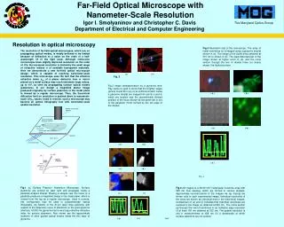
This study presents a groundbreaking far-field optical microscope capable of achieving nanometer-scale resolution by employing a dielectric droplet as a lens. Utilizing surface plasmon excitation and innovative imaging techniques, the system surpasses diffraction limits traditionally associated with optical microscopy. The microscope effectively captures high-resolution images of triplet nanohole arrays, demonstrating improvements in resolution through enhanced effective refractive indices. This design not only optimizes imaging but may also serve as a tool for nanolithography applications.

E N D
Far-Field Optical Microscope with Nanometer-Scale Resolution Regular microscope objective Dielectric droplet acting as a mirror Sample Focal point Surface plasmon-produced image Gold film Glass prism Laser illumination Igor I. Smolyaninov and Christopher C. Davis Department of Electrical and Computer Engineering Resolution in optical microscopy Fig.4 Resolution test of the microscope. The array of triplet nanoholes (c) is imaged using a glycerine droplet shown in (a). The image of the triplet array obtained at 515 nm is shown in (b). The least-distorted part of the image shown at higher zoom in (d), and the cross section through the line of double holes (e) clearly shows the triplet structure. The resolution of far-field optical microscopes, which rely on propagating optical modes, is widely believed to be limited because of diffraction to a value on the order of a half-wavelength l/2 of the light used. Although immersion microscopes have slightly improved resolution on the order of l/2n, the increased resolution is limited by the small range of refractive indices n of available transparent materials. Here we demonstrate a new far-field optical microscope design, which is capable of reaching nanometer-scale resolution. This microscope uses the fact that the effective refractive index neff of a planar dielectric lens or mirror placed on a metal surface may reach extremely large values, up to 103, as seen by propagating surface optical modes (plasmons). In our design a magnified planar image produced originally by surface plasmons in the metal plane is viewed by a regular microscope. Thus, the theoretical diffraction limit on resolution is pushed down to nanometer-scale l/2neff values. Used in reverse, such a microscope may become an optical lithography tool with nanometer-scale spatial resolution. ( a )( b ) Fig. 2 Fig.2 Image demagnification by a glycerine lens: Ray optics is used to show that the brighter edges (points A and B in (a)) of an artificial scratch inside a glycerine droplet are imaged into points a and b, which are located near the geometrically defined position of the focus (shown by the green dot in (b)) of the parabolic mirror formed by the left edge of the droplet. (a) (b) Fig.1 (a) Surface Plasmon Immersion Microscope: Surface plasmons are excited by laser light and propagate inside a parabolic-shaped droplet. Placing a sample near the focus of a parabola produces a magnified image in the metal plane, which is viewed from the top by a regular microscope. Used in reverse, this configuration may be used in subwavelength optical lithography. (b) Sketch of the Ar-ion laser lines positions with respect to the dispersion curve of plasmons on the gold-glycerine interface. At 502 nm glycerine has a very large effective refractive index for surface plasmons. Also shown are the approximate locations of other guided optical modes inside the thin layer of glycerine. Fig.3 2D images of a 30x30 mm2 rectangular nanohole array with 500 nm hole spacing, which are formed in various droplets. Approximate reconstructions of the images via ray tracing are shown next to each experimental image. Individual nanoholes of the array are shown as individual dots in the theoretical images. Comparison of (e) and (f) indicates that individual nanoholes are resolved in the image (e) obtained at 502 nm. The cross section (g) through the row of nanoholes in (e) indicates edge resolution of at least 100 nm obtained at 502 nm. The spatial resolution is lost in measurements at 458 nm (h) a wavelength at which surface plasmons are not excited.