Download
1 / 12
120 likes | 204 Views
This meeting aims to discuss emerging research architectures, memory technology assessment, and plan for the 2011 ERD chapter. Key topics include high-performance computing, alternative materials, and device production modeling. Major challenges with III-V MOSFETs will be addressed, such as gate dielectric issues, semiconductor interface passivation, and integration challenges. The proposal includes assessments on Ge and III-V materials, exploring nanowire FETs, graphene FETs, and carbon nanotube FETs. Recommendations will be made for advancing III-V and Ge technologies. Collaboration with ERD on device readiness and technology transfer to PIDS and FEP will be emphasized for future development.

E N D
DRAFT Beyond CMOS CTSG IRC Meeting December 15, 2009
Objectives Beyond CMOS CTSG IRC FxF Meeting Dec.15, 2009 • Follow up discussion of shared treatment of Alternate Channel Materials – Transfer to PIDS • Mention new Emerging Research Architectural planning underway for the 2011 ERD Chapter • Discuss ERD/ERM Workshops planned for 2010. • Memory Technology Assessment • Emerging Research Architectures • Emerging Research Devices – Hi Perf Computing • Emerging Research Devices – More than Moore
Production Ramp-up Model &Technology Cycle Timing Proposal [Example: III-V MOSFET Channel Replacement Materials] 100M Production Research Development 200K 10M 20K 1M 2K Transfer to PIDS/FEP (96-72mo Leadtime) Alpha Tool Beta Tool Product Tool 100K Volume (Wafers/Month) 200 10K 1st 2Cos. Reach Product First Tech. Conf. Device Papers Up to ~12yrs Prior to Product 20 1K 2 0 24 -96 -72 -24 -48 Months III/V Hi-m gate Example: 2011 2013 2015 2017 2019 2021 Source: 2009 ITRS – ERD/ERM/PIDS/FEP Proposal for Rev 3 Hutchby First Tech. Conf. Circuits Papers Up to ~ 5yrs Prior to Product
First Tech. Conf. Device Papers Up to ~12yrs Prior to Product III/V Hi-m gate Example: 2011 2013 2015 2017 2019 2021 Production Ramp-up Model &Technology Cycle Timing Proposal [Example: III-V MOSFET Channel Replacement Materials] Rev 4 Hutchby 100M Development Production Research 200K 10M 20K 1M 2K Transfer to PIDS/FEP (96-72mo Leadtime) Beta Tool Alpha Tool Product Tool 100K Volume (Wafers/Month) 200 10K 1st 2Cos. Reach Product 20 First Tech. Conf. Circuits Papers Up to ~ 5yrs Prior to Product 1K 2 0 24 -96 -72 -24 -48 Months Source: 2009 ITRS – ERD/ERM/PIDS/FEP Proposal for
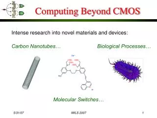
Major Challenges of III-V MOSFETs • High K Gate Dielectric • Passivation of High-K / III-V Semiconductor Interface • Integration of Ge and III-V Compound Semiconductor on Silicon • P-Channel III-V MOSFET or N-Channel Ge MOSFET
Issues Related to III-V MOSFETs • Impact of parasitics on I-V Characteristics • Effect of source resistance • Ballistic model for III-V FETs: role of Density-of-States • Ballistic FET I-V characteristics: InGaAs & Si • Quasi-Ballistic I-V characteristics: InGaAs & Si • Impact of parasitics on switching behavior • Estimation of switching behavior • Switching behavior of quasi-ballistic FETs: InGaAs & Si • Performance projection with scaling • Dimensional scaling • Supply voltage scaling • Drain leakage current
ERM ChallengesGe & III-V • Growth of low defect III-Vs on silicon • Co-integration of Ge & III-Vs • Ge dopant activation at higher temperatures • III-V doping of Ge • Growth of a high quality high κ dielectric on Ge & III-Vs • Passivation of the interface
ERD & ERM Alternate Channel Assessments • Ge p-FET • III-V n-FET • Ge p-FET & III-V n-FETs (Separate Assessment?) • Nanowire FETs • Graphene FETs • Carbon Nanotube FETs
III-V Ge Alternate Channel Partition Proposal ERM Materials, Interfaces & Process Issues & Challenges Critical Assessment of Materials & Integration Capabilities ERD Integrated Device Performance Assessment & Challenges (For different structures surface, buried channel, etc.) Critical Assessment of Device Performance FEP Potential Solution: SiGe P-FET with Si N-FET III-V & Ge Potential Solution Track III-V & Ge Issues PIDS III-V & Ge Potential Solution SiGe P-FET with Si N-FET Collaborate with ERD on device Readiness
ERD Recommendation ERD recommends to PIDS and FEP that we transfer the III-V and Ge Alternate Channel Materials Technology Element to PIDS and FEP in 2011
2009 Emerging Architectures • Benchmarking • Memory • Morphic • Thermodynamic