Toward Carbon Based Electronics Beyond CMOS Devices
170 likes | 453 Views
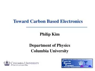
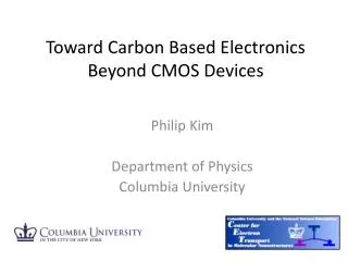
Toward Carbon Based Electronics Beyond CMOS Devices. Philip Kim Department of Physics Columbia University. End of the Road map: Quest for Beyond Si CMOS Era. Atomic orbital sp 2. Graphene. 0D. 1D. 2D. 3D. Carbon Nanotubes. Fullerenes (C 60 ). Graphite. p. s.

Toward Carbon Based Electronics Beyond CMOS Devices
E N D
Presentation Transcript
Toward Carbon Based ElectronicsBeyond CMOS Devices Philip Kim Department of Physics Columbia University
Atomic orbital sp2 Graphene 0D 1D 2D 3D Carbon Nanotubes Fullerenes (C60) Graphite p s SP2 Carbon: 0-Dimension to 3-Dimension
Material Platform: Low dimensional graphitic systems • 1-D: Carbon Nanotubes (since 1991) • 2-D: Graphene (since 2004) Device Concepts Conventional: (extended or ultimate) CMOS, SET Non-Conventional: Quantum Interference, Spintronics, valleytronics Outline: Carbon Based Electronics
E hole Energy kx' ky' electron ky kx Graphene : Dirac Particles in 2-dimension Band structure of graphene (Wallace 1947) Zero effective mass particles moving with a constant speed vF
Allowed states Semiconducting nanotube Metallic nanotube E E ky ky k1D k1D kx kx Single Wall Carbon Nanotube Eg ~ 0.8 ev / d (nm)
T = 250 K T = 250 K Resistance (kW) R (kW) R (kW) L (mm) le ~ 1 mm Length (mm) L (mm) Extremely Long Mean Free Path in Nanotubes Multi-terminal Device with Pd contact r = 8 kW/mm R ~ L R ~ RQ * Scaling behavior of resistance: R(L) Room temperature mean free path > 0.5 mm M. Purewall, B. Hong, A. Ravi, B. Chnadra, J. Hone and P. Kim, PRL (2007)
Isd (mA) -1.2 -0.8 -0.4 0 Vsd (V) Schottky barrier switching Ph. Avouris et al, Nature Nanotechnology 2, 605 (2007) Nanotube FET Band gap: 0.5 – 1 eV On-off ratio: ~ 106 Mobility: ~ 100,000 cm2/Vsec @RT Ballistic @RT ~ 300-500 nm Fermi velocity: 106 m/sec Max current density > 109 A/cm2
Thin body (1-2 nm) -> suppressed short channel effect • channel length ~ 10 nm has been demonstrated Javey et al. PRL (2004). • No-dangling bond at surface -> high k-dielectric compatible Cg ~ CQ can be attainable; small RC, low energy Appenzeller et al., PRL (2002) Advantages of CNTFET • Novel architecture -> • Band-to-band tunneling FET: • subthreshold slop ~ 40 meV/dB @RT
IBM, Avouris group graphene Aligned growth of Nanotubes Rodgers, UIUC Nanotube Ring Oscillators Artistic dream (DELFT) Nanotube Electronics: Challenges Pros: High mobility High on-off ratio High critical current density Small channel length Small gate capacitance Large Fermi velocity Con: Controlled growth
Discovery of Graphene Large scale growth efforts: CVD, MBE, chemical synthesis
factor 4 / year Growth of Graphene Research Number of Graphene Publications on arXiv /month Dec 04 Dec 05 Dec 06 Dec 07 Aug 05 Aug 06 Aug 07 Jun 08 Oct 04 Oct 05 Oct 06 Oct 07 Feb 05 Jun 05 Feb 06 Jun 06 Feb 07 Jun 07 Feb 08 Apr 05 Apr 06 Apr 07 Apr 08
GaAs HEMT Mechanically exfoliated graphene Modulate Doped GaAs: Pfeiffer et al. TC17 Mobility (cm2/V sec) TC12 Scattering Mechanism? TC145 • Ripples • Substrate (charge trap) • Absorption • Structural defects TC130 n (1012 cm-2) Graphene Mobility Tan et al. PLR (2007)
SEM image of suspended graphene graphene Enhanced Room Temperature Mobility of Graphene Graphene mobility: > 100,000 cm2/Vsec @ room temperature after annealing Mobility (cm2/V sec) before annealing unsuspended best Density ( 1012 cm-2) High mobility materials have been under intensive research as an alternative to Silicon for higher performance mobility: Si (1,400 cm2/Vsec), InSb (77,000 cm2/Vsec)
Graphene FET characteristics • Low temperature direct atomic layer deposition (ALD) of HfO2 as high-κ gate dielectric • Top-gate electrode is defined with a final lithography step. • I-V measurements at two different back gate voltages show a distinct “kink” for different top-gate voltages • Transconductance can be as high as gm = 328μS (150μS/μm) • Poor on-off ratio: ~ 5-10 due to zero gap in bulk Meric, Han, Young, Kim, and Shepard, Nature Nanotech (2008)