Download
1 / 17
190 likes | 385 Views
International Symposium on Compound Semiconductors 2011. InGaAs/InP DHBTs in a planarized, etch-back technology for base contacts. Vibhor Jain , Evan Lobisser, Ashish Baraskar, Brian J Thibeault, Mark Rodwell ECE Department, University of California, Santa Barbara, CA 93106-9560

E N D
International Symposium on Compound Semiconductors 2011 InGaAs/InP DHBTs in a planarized, etch-back technology for base contacts Vibhor Jain, Evan Lobisser, Ashish Baraskar, Brian J Thibeault, Mark Rodwell ECE Department, University of California, Santa Barbara, CA 93106-9560 D Loubychev, A Snyder, Y Wu, J M Fastenau, W K Liu IQE Inc., 119 Technology Drive, Bethlehem, PA 18015 vibhor@ece.ucsb.edu, 805-893-3273
Outline • HBT Scaling Laws • Refractory base ohmics • Fabrication • DHBT – Epitaxial Design and Results • Summary
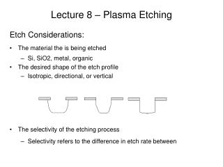
We Wbc Tb Tc (emitter length Le) Bipolar transistor scaling laws To double cutoff frequencies of a mesa HBT, must: Keep constant all resistances and currents Reduce all capacitances and transit delays by 2 Epitaxial scaling Lateral scaling Ohmic contacts
InP bipolar transistor scaling roadmap Design Performance Rodwell, Le, Brar, Proceedings of IEEE, 2008
TEM by E Lobisser Ashish Baraskar Contact diffusion 15 nm Pd diffusion • Pd contacts diffuse in base (p-InGaAs) • Contact resistance ↑ for thin base • Limits base thickness • Scaling Limitation 100 nm InGaAs grown in MBE Need for non-diffusive, refractory base metal
Ashish Baraskar et al., EMC 2010 Refractory base ohmics Ashish Baraskar et al., Int. MBE 2010 Refractory metal base contacts Require a blanket deposition and etch-back process
Emitter process flow Mo contact to n-InGaAs for emitter W/TiW/SiO2/Cr dep SF6/Ar etch SiNx Sidewall SiO2/Cr removal InGaAs Wet Etch Second SiNx Sidewall InP Wet Etch W/TiW interface acts as shadow mask for base lift off Collector formed via lift off and wet etch BCB used to passivate and planarize devices
Base process flow – I Blanket refractory metal PR Planarization Isotropic Dry etch of metal Removes any Emitter-Base short Ti0.1W0.9 Ti0.1W0.9 W W PR Mo Mo InGaAs InGaAs InP InP p+ InGaAs Base p+ InGaAs Base
Ti0.1W0.9 Ti0.1W0.9 SiNx W W Mo Mo InGaAs InGaAs InP InP p+ InGaAs Base p+ InGaAs Base Base process flow – II Lift-off Ti/Au Low base metal resistance Blanket SiNx mask Etch base contact metal in the field
Base Planarization Planarization: Emitter projecting from PR for W dry etch Etch Back Planarization Boundary
Epitaxial Design Vbe = 1 V, Vcb = 0.7 V, Je = 25 mA/mm2 Low Base doping Good refractory ohmics not possible Pd/W contacts used
Results - DC Measurements Common emitter I-V @Peak ft,fmax Je = 17.9 mA/mm2 P = 30 mW/mm2 BVceo = 2.4 V @ Je = 1 kA/cm2 β = 26 JKIRK = 21 mA/mm2 Gummel plot
1-67 GHz RF Data Ic = 22.4 mA Vce = 1.67 V Je = 17.9 mA/mm2 Vcb = 0.7 V Single-pole fitto obtain cut-off frequencies
Equivalent Circuit Rex = 6 Wmm2 Hybrid-p equivalent circuit from measured RF data
TEM Large undercut in base mesa Pd/W adhesion issue High Rbb Low fmax 0.1 mm Pd/W adhesion issue Large mesa undercut
Summary • Demonstrated a planarized, etch back process for refractory base contacts • Demonstrated DHBTs with peakft/ fmax = 410/690 GHz • Higher base doping, thinner base and refractory base ohmics needed to enable higher bandwidth devices
Thank You Questions? This work was supported by the DARPA THETA program under HR0011-09-C-006. A portion of this work was done in the UCSB nanofabrication facility, part of NSF funded NNIN network and MRL Central Facilities supported by the MRSEC Program of the NSF under award No. MR05-20415