Download
1 / 13
130 likes | 294 Views
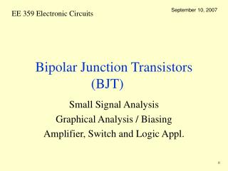
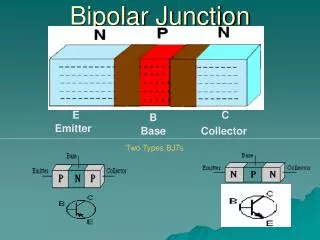
Bipolar Junction. E. C. B. Emitter. Base. Collector. Two Types BJTs. Bipolar Junction Transistor. Bipolar Junction Transistor.

E N D
Bipolar Junction E C B Emitter Base Collector Two Types BJTs
Bipolar Junction Transistor Note that the two symbols are subtly different. The vertical line represents the base (B), the angular line with the arrow on it represents the emitter (E), and the other angular line represents the collector (C). The direction of the arrow on the emitter distinguishes (graphically) the NPN from the PNP transistor. If the arrow points in, (Points iN) the transistor is a PNP. On the other hand if the arrow points out, the transistor is an NPN (Not Pointing iN).
Bipolar Junction Transistor Some of the basic properties exhibited by a Bipolar Transistor are immediately recognizable as being diode-like. However, when the 'filling' of the sandwich is fairly thin some interesting effects become possible that allow us to use the Transistor as an amplifier or a switch. To see how the Bipolar Transistor works we can concentrate on the NPN variety.
Energy Levels of NPN Figure 1 shows the energy levels in an NPN transistor when we aren't externally applying any voltages. We can see that the arrangement looks like a back-to-back pair of PN Diode junctions with a thin P-type filling between two N-type slices of 'bread'. In each of the N-type layers conduction can take place by the free movement of electrons in the conduction band. In the P-type (filling) layer conduction can take place by the movement of the free holes in the valence band. However, in the absence of any externally applied electric field, we find that depletion zones form at both PN-Junctions, so no charge wants to move from one layer to another.
Reverse Bias Base NPN Consider now what happens when we apply a moderate voltage between the Collector and Base parts of the transistor. The polarity of the applied voltage is chosen to increase the force pulling the N-type electrons and P-type holes apart. (i.e. we make the Collector positive with respect to the Base.) This widens the depletion zone between the Collector and base and so no current will flow. In effect we have reverse-biased the Base-Collector diode junction. The precise value of the Base-Collector voltage we choose doesn't really matter to what happens provided we don't make it too big and blow up the transistor! So for the sake of example we can imagine applying a 10 Volt Base-Collector voltage
Forward Vbe NPN When we apply a relatively small Emitter-Base voltage whose polarity is designed to forward-bias the Emitter-Base junction. This 'pushes' electrons from the Emitter into the Base region and sets up a current flow across the Emitter-Base boundary. As a result the electrons which get into the Base move swiftly towards the Collector and cross into the Collector region. Hence we see a Emitter-Collector current whose magnitude is set by the chosen Emitter-Base voltage we have applied. To maintain the flow through the transistor we have to keep on putting 'fresh' electrons into the emitter and removing the new arrivals from the Collector. Hence we see an external current flowing in the circuit
Active Region of BJT N P N
Biasing Effect as an amplifier Low value Vbe medium value Vbe High value Vbe
Inverting and Non-Inverting Inverting Output Input Non-Inverting Output