Download
1 / 24
240 likes | 262 Views
Understand the basics of noise in semiconductor devices and the importance of amplifiers for detector systems. Learn about intrinsic and extrinsic noise sources, preamplifiers, amplifier types, noise minimization, and noise calculations. Explore key concepts such as impulse response, transfer functions, and noise sources normalization. Gain insights into noise properties in amplifier systems and the significance of calibration for accurate measurements in semiconductor applications.

E N D
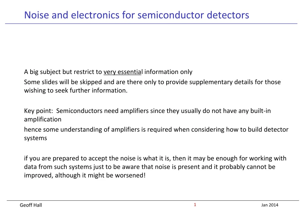
Noise and electronics for semiconductor detectors A big subject but restrict to very essential information only Some slides will be skipped and are there only to provide supplementary details for those wishing to seek further information. Key point: Semiconductors need amplifiers since they usually do not have any built-in amplification hence some understanding of amplifiers is required when considering how to build detector systems if you are prepared to accept the noise is what it is, then it may be enough for working with data from such systems just to be aware that noise is present and it probably cannot be improved, although it might be worsened! Geoff Hall
What is NOISE? A definition: Any unwanted signal obscuring signal to be observed two main origins EXTRINSIC NOISE examples... pickup from external sources unwanted feedback RF interference from system or elsewhere, power supply fluctuations ground currents small voltage differences => currents can couple into system may be hard to distinguish from genuine signals but AVOIDABLE Assembly & connections, especially to ground, are important INTRINSIC NOISE Fundamental property of detector or amplifying electronics Can’t be eliminated but can be MINIMISED Noise Geoff Hall
Preamplifier usually designed with noise as an important consideration preamplifier pulse shape is long duration with short, sharp peak so modify it with shaper to optimise signal to noise generate a more practical pulse shape, avoiding pile-up the first (pre-) amplifier is the most important part of the system for noise The system noise can be calculated once sources are understood relies on Campbell’s theorem and summation over bandwidth Noise in amplifier systems • VFE systems comprise • preamplifier - with noise sources • shaping amplifier or other filter Geoff Hall
Current sensitive - common for photodiode signals vout ≈ -iinRf signals follow input current, ie fast response but not lowest noise Charge sensitive amplifier Ideally, simple integrator with Cf but need means to discharge capacitor - large Rf Simple integrator vout ≈ -Q/Cf with feedback resistor Rf vout(t) ≈ -(Q/Cf)exp(-t/t) t = RfCf Omit most – just be aware that different amplifier types have different noise properties and are not interchangeable Preamplifier types Geoff Hall
If noise sources are defined, their impact can be calculated pulse shaping is most common sampling an amplifier signal can produce equivalent behaviour Useful point of comparison: CR-RC filter Signal processing series (Rs) parallel (I) numerical result for many cases Geoff Hall
An approximate numerical value using CR-RC filter, ignoring 1/f noise ie I = 1nA t = 1µs ENCp ≈ 100e Rs = 10Ω C = 10pF t = 1µs ENCs ≈ 24e Some numerical values Geoff Hall
Noise vs technology after V. Radeka peaking time Geoff Hall
System noise can be computed with knowledge of impulse response and noise sources s2 ~ en2 C2∫ [h'(t)]2 dt + in2∫[h(t)]2 dt provided noise sources en & in are white properly normalise to signal of unit amplitude Impulse response = output of system following fast -like input signal h(t) Noise calculations • Summary of principles • integrate signal spectrum over bandwidth • integrate noise in quadrature over bandwidth • computation can be done in time or frequency domain but simplifications are often possible Geoff Hall
Most amplifying systems designed to be linear S(t) = S1(t) + S2(t) +S3(t) + … Impulse response h(t) = response to d Transfer function H(w) = vout(w)/vin(w) = ∫-∞∞ h(t).e-jwtdt ie impulse response h(t) and transfer function H(w) are Fourier pair In a linear system, if random impulses occur at rate n average response <v> = n ∫-∞tobsh(t)dt variance s2 = n∫-∞tobs[h2(t)]dt so s2 = n ∫-∞∞ h2(t) dt = n∫-∞∞|H(w)|2df Omit Campbell’s theorem i.e. sum all pulses preceding time, tobs, of observation Geoff Hall
Combine uncorrelated noise sources in quadrature e2tot = e12 +e22 +e32 + … + in2R2 +... follows from Campbell's theorem consider as combinations of gaussian distributions First stage of amplifier dominates noise originates at input input transistor is most important - defines noise in most cases Noise is independent of amplifier gain or input impedance so noise can be referred to input In real systems both are approximations - but normally good ones so often sufficient to focus on input device Omit "Rules" of low noise amplifier systems Geoff Hall
Systems need to be calibrated: ENC is the signal magnitude which produces an output amplitude equal to the r.m.s. noise ideally measure in some absolute units - e, coul, keV(Si),… rather than ADC channels to calibrate inject charge and look at result eg x-ray signal of known size or electronic test pulse preferably in-situ measure Vout for known Qin Qtest = CtestVtest = Ne Equivalent Noise Charge Geoff Hall
Thermal noise Quantum-statistical phenomenon; carriers in constant thermal motion macroscopic fluctuations in electrical state of system Typically associated with input transistor or resistive components Shot noise Random fluctuations in DC current flow Typically associated with sensor 1/f noise commonly associated with interface states in MOS electronics Luckily, less important for high speed electronics Noise sources Geoff Hall
Poisson fluctuations of charge carrier number eg arrival of charges at electrode in system - induce charges on electrode quantised in amplitude and time Examples electrons/holes crossing potential barrier in diode or transistor electron flow in vacuum tube < in2> = 2qI.∆f WHITE (NB notation e = q) I = DC current Shot noise gaussian distribution of fluctuations in i Geoff Hall
Einstein (1906) , Johnson, Nyquist (1928) Mean voltage <v> = 0 Variance <v2> = 4kT.R.∆f ∆f = observing bandwidth s(v) = √<v2> = 1.3 10-10 (R.∆f)1/2 volts at 300K e.g. R = 1MΩ ∆f = 1Hz s(v) = 0.13µV Noise power = 4kT.∆f independent of R & q independent of f - WHITE Circuit representations Noise generator + noiseless resistance R Spectral densities mean square noise voltage or current per unit frequency interval wV(f) = 4kTR (voltage) wI(f) = 4kT/R (current) Just note that this is needed to do calculations Thermal noise gaussian distribution of fluctuations in v Geoff Hall
Reminder of basic FET physics bias “metal” gate to deplete substrate beyond a certain threshold voltage, substrate does not deplete deeper instead “inversion layer” created CMOS transistor • Inversion layer • extremely shallow, at oxide-silicon interface • carriers mobile in applied field • Transistor operation • Modulation of source-drain current via Vgate L Geoff Hall
Gate shot noise is negligible insulating gate and no current Thermal noise voltage from channel g= excess noise factor ~ 1 Transconductance Cox = eox /tox W/L = transistor width/length 1/f noise usually unimportant (for LHC) Implications To achieve low noise, aim for large W/L and large (tolerable) IDS but Camp = CoxWL and require capacitance matching: Camp ≈ Cdet/3 Mobility is also T dependent, influencing noise and speed µ(T) ~ T-3/2 Noise in MOS circuits Omit C = capacitance T = temperature ∆f = bandwidth µ = mobility (v/E) Geoff Hall
pMOS preferred for lower 1/f noise Noise spectra • 3dB bandwidth • eg LHC ∆f3db = 2.6 - 15.4MHz • CR-RC pulse shaping • = 25ns • or 1/f noise might be an issue Geoff Hall
Basic sources are Shot noise in ICic2 = 2eIC∆ƒ Shot noise in IBib2 = 2eIB∆ƒ Thermal noise in base & contacts eb2 = 4kT . rbb' .∆ƒ Reconfigure so that noise sources are external which then shows that i2nand e2n are correlated, ie can’t reduce both simultaneously so achievable range of noise is limited and happens to provide best performance for high speed applications however bipolar noise determined mainly by currents so easy to estimate Bipolar transistor noise Omit Geoff Hall
Alternative to pulse shaping filters based on summation easy to implement in several technologies eg. typically switched capacitor filters but also delay-line or digital possible beware of extra noise issues based on sample & hold e.g. double correlated sampling Switched capacitor design convenient for CMOS accurate capacitances (ratios) MOSFET switches Time variant filters - sampling delay line DCS MX ASIC DCS Geoff Hall
How to calculate noise of time variant systems? What output is produced at Tm by impulse at time t? consider all t - defines weighting function Time invariant filter w(t) is mirror image of h(t) Noise calculation ENC2 = en2 C2∫ [w'(t)]2dt + in2∫[w(t)]2dt Weighting function Omit Geoff Hall
Sample & hold method initially switches S0 B1 B2 open, S1 S2 closed switch S0 is Reset Vout = output from charge sensitive preamplifier open S1 : preserves Vout on C1 after time ∆t open S2 : preserves Vout on C2 then, close B1 and B2: output A = V1 - V2 reset preamp later need to know when signal will arrive! Vout Double correlated sampling Geoff Hall
Example of time-variant filter.. Convolution of pulse shape with gate w(t) = h(t) * ggate(t) (ignoring t reflection) examples CR-RC pulse + integrating ADC Tgate << t Tgate = 5t Tgate >> t similar to peak sensing ADC gated at peak! new, wider weighting function recompute noise integrals ADC may change filtering and increase or decrease noise Geoff Hall
Eventually need to convert signal to a number quantisation (rounding) of number = noise source the more precise the digitisation, the smaller the noise After digitisation all that is known is that signal was between -∆/2 and ∆/2 <x> = ∫x.p(x).dx/∫p(x).dx s2 = <x2> = ∫x2.p(x).dx /∫p(x).dx ∫p(x).dx = ∫-∆/2∆/2 dx = [x] -∆/2∆/2 = ∆ ∫x2.p(x).dx = ∫-∆/2∆/2 x2.dx = [x3/3] -∆/2∆/2 = 2∆3/24 so s2 = ∆2/12 ie statistical noise which is proportional to digitisation unit Digitisation noise Geoff Hall
When did signal cross threshold ? noise causes “jitter” Dt = snoise/(dV/dt) compromise between bandwidth (increased dV/dt) noise (decreased bandwidth) limits systems where preamplifier pulse used to generate trigger eg x-ray detection typical preamp response V = Vmax(1-e-t/trise) so ∆t ≈ snoisetrise/ Vmaxt << t Time measurements and noise Geoff Hall