Photolithography
220 likes | 507 Views
Photolithography. Why Photolithography. Low cost IC manufacturing Due to large number of lithographic steps needed in IC manufacturing, lithography typically accounts for about 30% of cost of manufacturing. Photolithography cost minimize result in low cost IC

Photolithography
E N D
Presentation Transcript
Why Photolithography • Low cost IC manufacturing • Due to large number of lithographic steps needed in IC manufacturing, lithography typically accounts for about 30% of cost of manufacturing. • Photolithography cost minimize result in low cost IC • Ultra miniaturized electronic device manufacturing • With photolithography ultra miniaturized IC manufacturing is possible resulting in miniature electronic device
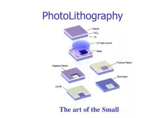
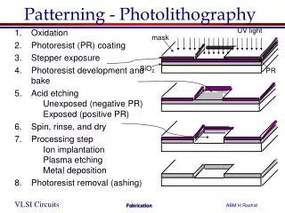
Basic Process of Lithography • Substrate • Base layer consists of either glass, silica etc. • Depositing Film • A thin layer of SiO2 coated at the top of substrate • Pattern the Film • Imaging the pattern from the template to the film • Etching • Removing the unnecessary part of the film and keeping the required pattern. • Can be performed using different chemicals( acids)
Procedure of Photolithography • Cleaning(Surface Preparation) • Chemicals like H2O2, acetone are used to clean the surface of substrate to clear from dust particle or any contaminant. • A layer of silicon is placed on the wafer or substrate to act as masking film • Photoresist • Viscous solvent have binding and adhesive property • Photoactive compound that activates in presence of light • Activate at the wavelength of the light that we plan to use • Coated with the thickness of 0.5 to 2.5 micrometerat the top of SiO2 layer using spin coating which runs typically 1200 to 4800 rpm for 30 to 60 sec. • Types • Positive photoresist • Area exposed to light becomes soluble in chemical while developing • Negative photoresist • Area exposed to light get polymerize and remains the same and area that is not exposed becomes soluble • Commonly used negative photoresist is SU8
Contd.. • Soft Bake • After coating, the resulting resist film will contain between 20 – 40% by weight solvent. At room temperature, an unbaked photoresist film will lose solvent by evaporation, thus changing the properties of the film with time. • Film thickness is reduced • Adhesion is improved • The film becomes less tacky and thus less susceptible to particulate contamination • Dry off excessive photoresist solvent so that it becomes stable at room temperature. • Exposed at a temperature of 90 degrees to 100 degrees for 30 sec. • Align and Exposure • The basic principle behind the operation of a photoresist is the change in solubility of the resist in a developer upon exposure to light • To imprint the correct pattern in the wafer mask alignment is required. If the alignment of mask is not accurate, the printed pattern will not be correct.
Contd.. • Developing • Chemical used to remove the unwanted photoresist. These are mostly aqueous base chemical as developer • Generally used tetra-methyl ammonium hydroxide (TMAH) as developer • Hard Bake • The hard bake is used to harden the final resist image so that it will withstand the harsh environments of implantation or etching. • The high temperatures used is 120°C - 150°C. • If the temperature used is too high, the resist will flow causing degradation of the image. • Etching • This removes the unwanted SiO2 layer • Normally acids are used for this purpose • Stripping • Stripping out unwanted photoresist material.
Capacity Enhancement • The ability to project clear image(Projection Printing) of small feature in wafer is dependent on wavelength and ability of capture lens to capture the diffraction light. • Smaller feature uses smaller wavelength of light • As per light energy required, various wavelength with various light intensity can be used • UV 365 nm – 436 nm • Deep UV(DUV) 157 nm – 250 nm • Extreme UV(EUV) 11 nm – 14 nm • X-ray <10 nm
Resolution • The achievable, repeatable minimum feature size • Determined by the wavelength of the light and the numerical aperture of the system. The resolution can be expressed as
Summary • Photolithography uses three basic process steps to transfer a pattern from a mask to a wafer: coat, develop, expose. • The pattern is transferred into the wafer’s surface layer during a subsequent process. • Capacity enhancement is dependent on wavelength and numerical aperture.