Download
1 / 36
1.52k likes | 3.33k Views
CHAPTER 1: INTRODUCTION TO OPERATIONAL AMPLIFIERS. Objectives. Describe basic op-amp characteristics. Discuss op-amp modes and parameters. Explain negative feedback. Analyze inverting, non-inverting, voltage follower and inverting op-amp configurations. BASIC OP-AMP. Symbol and Terminals.

E N D
Objectives • Describe basic op-amp characteristics. • Discuss op-amp modes and parameters. • Explain negative feedback. • Analyze inverting, non-inverting, voltage follower and inverting op-amp configurations.
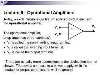
Symbol and Terminals • A standard operational amplifier (op-amp) has; • Vout is the output voltage, • V+ is the non-inverting input voltage, • V- is the inverting input voltage. • Typical op-amp operates with 2 dc supply voltages, • +ve supply. • –ve supply. Figure 1a: Symbol Figure 1b: Symbol with dc supply connections
An op amp is an active circuit element designed to perform mathematical Operations of addition, subtraction, multiplication, division, differentiation, and integration. 741 general purpose op-amp made by Fairchild Semiconductor
Operational Amplifiers The op amp is built using VLSI techniques.The circuit diagram of an LM 741 from National Semiconductor is shown below. V+ Vin(-) Vo Vin(+) Taken from National Semiconductor data sheet as shown on the web. Internal circuitry of LM741. V-
_ Vin AvVin Zin=∞ Zout=0 Av=∞ + The Ideal Op-Amp • The ideal op-amp has; • Infinite voltage gain. • Infinite bandwidth. • Infinite input impedance • zero output impedance. • The input voltage, Vin appears between the two input terminal. • The output voltage is AvVinas indicated by the internal voltage source symbol. Figure 2a: Ideal op-amp representation
_ Zin Vin AvVin Zout + The Practical Op-Amp • Characteristic of a practical op-amp are; • Very high voltage gain. • Very high input impedance. • Very low output impedance. • Wide bandwidth. Figure 2b: Practical op-amp representation
Input Signal Modes A) Single-Ended Input • Operation mode; • One input is grounded. • The signal voltage is applied only to the other input. • When the signal voltage is applied to the inverting input, • an inverted amplified signal voltage appears at the output. (figure 3a) _ + Figure 3a
When the signal voltage is applied to the noninverting input with the inverting input grounded, • a noninverted amplified signal voltage appears at the output. (figure 3b) _ + Figure 3b
B) Differential Input • Operation mode; • Two opposite-polarity (out-of-phase) signals are applied to the inputs • This type of operation is also referred to as double-ended. • The amplified difference between the two inputs appears on the output. _ + Figure 3c
C) Common-Mode Input • Operation mode • Two signal voltages of the same phase, frequency and amplitude are applied to the two inputs. (figure 3d) • When equal input signals are applied to both inputs, they cancel, resulting in a zero output voltage. • This action is called common-mode rejection. • Means that this unwanted signal will not appear on the output and distort the desired signal. _ + Figure 3d
Common-Mode Rejection Ratio • Desired signals can appear on only • one input or • with opposite polarities on both input lines. • These desired signals are • amplified and appear on the output. • Unwanted signals (noise) appearing with the same polarity on both input lines are • essentially cancelled by the op-amp and do not appear on the output. • The measure of an amplifier’s ability to reject common-mode signal is called • CMRR (common-mode rejection ration). • Ideally, op-amp provides • a very high gain for desired signal (single-ended or differential) • zero gain for common-mode signal.
The higher the open-loop gain with respect to the common-mode gain, • the better the performance of the op-amp in terms of rejection of common-mode signals. • Therefore; where Aol = open-loop voltage gain Acm = common-mode gain • The higher the CMRR, the better. • A very high value of CMRR means that • the open-loop gain, Aol is high and • the common-mode gain, Acm is low. • The CMRR expressed in decibels (dB) is
Open-Loop Voltage Gain • Open-loop voltage gain, Aol of an op-amp • is the internal voltage gain of the device • represents the ration of output voltage to input voltage when there are no external components. • The open-loop voltage gain is set entirely by the internal design. • Open-loop voltage gain can range up to • 200,000 and is not a well-controlled parameter. • Data sheet often refer to the open-loop voltage gain as • the large-signal voltage gain.
Example 1 A certain op-amp has an open-loop voltage gain of 100,000 and a common-mode gain of 0.2. Determine the CMRR and express it in decibels. Answer: a) 500,000 b) 114dB
Common-Mode Input Voltage Range • All op-amp have limitation on the range of voltages over which they will operate. • The common-mode input voltage range is • the range of input voltages which when applied to both inputs will cause clipping or other output distortion. • Many op-amp have common-mode input ranges of • ±10V with dc supply voltages of ±15V.
I1 V1 _ I2 Vout + V2 Input Bias Current • The input bias current is • the dc current required by the inputs of the amplifier to properly operate the first stage. • By definition, the input bias current is • the average of both input currents and is calculated as; Figure 4a: Input bias current is the average of the two op-amp input currents.
Input Impedance • Two basic ways of specifying the input impedance of an op-amp are • Differential. • Common-mode. • Differential input impedance is • the total resistance between the inverting and the noninverting input. • Measured by determining the change in bias current for a given change in differential input voltage. ZIN(d) Figure 4b: Differential input impedance
Common-mode input impedance is • the resistance between each input and ground. • Measured by determining the change in bias current for a given change in common-mode input voltage. ZIN(cm) Figure 4c: Common-mode impedance
Output Impedance • The output impedance is • the resistance viewed from the output terminal of the op-amp as indicated in figure 4d Zout Figure 4d: Op-amp output impedance
Slew Rate • What is slew rate? • The maximum rate of change of the output voltage in response to a step input voltage. • Is dependent upon the high-frequency response of the amplifier stages within the op-amp. • Is measured with an op-amp connected as shown in figure 4e Figure 4e: Test circuit
Vin 0 +Vmax Vout -Vmax ∆t • A pulse is applied to the input, the output voltage is measured as indicated in figure 4f. • The width of the input pulse must be sufficient • to allow the output to slew from its lower limit to its upper limit. • A certain time interval ∆t, is required for the output voltage • to go from its lower limit –Vmax to its upper limit +Vmax, once the input step is applied. Figure 4f: Step input voltage and the resulting output voltage
The slew rate is expressed as Where ∆Vout = +Vmax-(-Vmax). • The unit is volts per microsecond (V/μs).
Vout(V) 10 9 0 t -9 -10 2μs 12μs Example 2 The output voltage of a certain op-amp appears as shown in figure below in response to a step input. Determine the slew rate. Answer: 1.8 V/us
OP-AMPS WITH NEGATIVE FEEDBACK • Negative feedback is a process whereby a portion of the output voltage returned to the input with a phase angle opposed the input signal • Advantages: • Higher input impedance • More stable gain • Improved frequency response • Lower output impedance • More linear operation
Closed-Loop Voltage Gain, Acl • The closed-loop voltage gain is • the voltage gain of an op-amp with external feedback. • The amplifier configuration consists of • the op-amp • an external negative feedback circuit that connects the output to the inverting input. • The closed-loop voltage gain is determined by • the external component values and can be precisely controlled by them.
Noninverting Amplifier Figure 5: Noninverting amplifier • Noninverting amplifier is • an op-amp connected in a closed-loop with a controlled amount of voltage gain is shown in figure 5. • The input signal is applied to • the noninverting (+) input. • The output is applied back to • the inverting (-) input through the feedback circuit (closed loop) formed by the input resistor Ri and the feedback resistor Rf. Feedback network
This creates negative feedback as follows. • Resistor Ri and Rf form a voltage divider circuit, which reduces Vout and connects the reduced voltage Vf to the inverting input. • The feedback voltage is expressed as • The closed-loop gain of the noninverting (NI) amplifier is • Where • Therefore;
Example 3 Determine the gain of the amplifier in figure below. The open-loop voltage gain of the op-amp is 100,000. 100kΩ 4.7kΩ Answer: 22.3
Voltage-Follower • The voltage-follower configuration is a special case of the noninverting amplifier • where all the output voltage is fed back to the inverting (-) input by a straight connection. (figure 6) • The straight feedback connection has a voltage gain of 1 (no gain). • The closed-loop voltage gain of a noninverting amplifier is 1/B. Figure 6: Op-amp voltage-follower
Since B=1, for a voltage-follower, • the closed-loop voltage gain of the voltage follower is Acl(VF)=1 • The most important features of the voltage-follower configuration are • very high input impedance • very low output impedance. • These features make it a nearly ideal buffer amplifier for the • interfacing high-impedance sources • low-impedance loads.
Inverting Amplifier • Inverting amplifier • An op-amp connected with a controlled amount of voltage gain. (figure 7) • The input signal is applied through a series input resistor Ri to the inverting (-) input. • The output is fed back through Rf to the same input. • The noninverting (+) input is grounded. Aol Figure 7: Inverting Amplifier
For inverting amplifier • The closed-loop voltage gain is the ratio of the feedback resistance (Rf) to the input resistance (Ri). • This gain is independent of the op-amp’s internal open-loop gain. • Thus, the negative feedback stabilizes the voltage gain. • The negative sign indicates inversion. Therefore;
Example 4 Given the op-amp configuration in figure below, determine the value of Rf required to produce a closed-loop voltage gain of -100. 2.2kΩ Aol Answer: 220 kΩ