Experiment (ZTO)
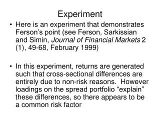
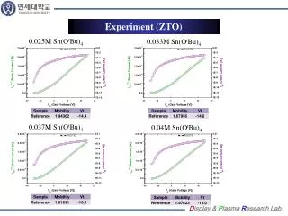
Experiment (ZTO). 0.025M Sn ( O t Bu ) 4. 0.033M Sn ( O t Bu ) 4. 0.037M Sn ( O t Bu ) 4. 0.04M Sn ( O t Bu ) 4. Experiment (ZTO). ZnOAc,300°C. ( Zn+Sn )OAc,300°C. ZnOAc,350°C. ( Zn+Sn )OAc,350°C. Experiment (Cs-In 2 O 3 ). Cs 1%. Cs 2%. Defects. M-O-M. O1s peaks. Cs 3%. Cs 4%.

Experiment (ZTO)
E N D
Presentation Transcript
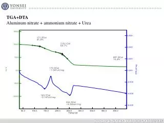
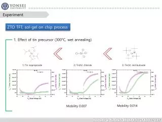
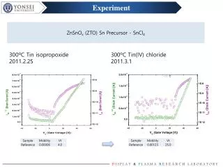
Experiment (ZTO) 0.025M Sn(OtBu)4 0.033M Sn(OtBu)4 0.037M Sn(OtBu)4 0.04M Sn(OtBu)4
Experiment (ZTO) ZnOAc,300°C (Zn+Sn)OAc,300°C ZnOAc,350°C (Zn+Sn)OAc,350°C
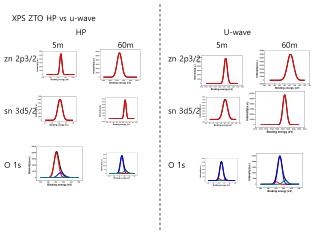
Experiment (Cs-In2O3) Cs 1% Cs 2% Defects M-O-M O1s peaks Cs 3% Cs 4%
Experiment (Cs-In2O3) Cs3d peaks In3d peaks Cs 4% Cs 3% Cs 2% Cs 1%
Experiment (Cs-In2O3) Cs 1% Cs 2% Cs 3% Cs 4% 2Cs(NO3) → 2Cs(NO2) + O2 At 400°C Precursor changed to CsCl
Experiment (Al2O3) Thickness : 10.7nm Leakage current : 13.6nA/cm2 at 1MV/cm Capacitance : 264 nF/cm2
Experiment (Al2O3) * Leakage current at 1MV/cm Al2O3 Al2O3 C HfO2 C
Experiment (Al2O3-urea) * Leakage current at 0.1MV/cm * k~8 Al2O3 x1 Al2O3 x2 Al2O3 x3
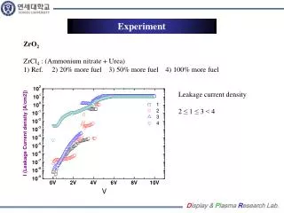
Experiment ZrO2 ZrCl4 : (Ammonium nitrate + Urea) 1) Ref. 2) 20% more fuel 3) 50% more fuel 4) 100% more fuel Leakage current density 2 ≤ 1 ≤ 3 < 4
Experiment Al2O3Acac Al2O3 ref. Al2O3 Urea HfO2 ref. HfO2 Urea
Self-assembled viral LC film M13 virus – rod like shape Its protein shell – has dipole and piezoelectricity ( + terminated C , - terminated N ) Assembled in nematic or smectic phase ~2pm/V of piezoelectric response
Self-assembled droplet Metal ink droplet Hydrophobic treatment & Topology effect Ink-jetted droplet is divided and make pattern Nanorod self-assembly on patterned substrate (Geometrically or surface energy) Using flow on substrate (Nanorod orientation & location)
Origin of In2O3 carrier Oxygen vacancy model is valid for ZnO By hybrid DFT + GW model, In2O3 – VO : deep donor (Ionization is not easy) Surface VO : donor-like surface defect → Carrier density increases as thickness decreases (Calculation based on crystalline In2O3) explaining our observations: high temperature → crystallization → Off-current increasing
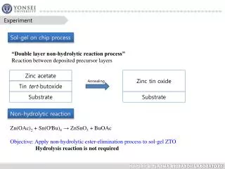
Solvent-free sol-gel 800nm thickness passivation film by 1-time spin coating (4500RPM) Non-hydrolytic sol-gel Moderate reaction rate Low curing temperature and No volume shrinkage
Nanoparticle based TFT ZnO nanoparticle Optimum particle size ~4nm (0.88cm2/Vs) Precursor ligands: Acetate (short) – semiconducting NPs Hexanoate(long) – dielectric NPs Post plasma treatment PL Defect peak reduced Mobility up to ~20cm2/Vs In2O3nanoparticle Particle size ~20nm 400C annealing to remove stabilizer 4.5cm2/Vs with ion gel dielectric
CBD-based CdS TFT Chemical bath deposition: deposition temperature < 100C Fully photolithographically patterned device Mobility : 8 cm2/Vs before annealing 11 cm2/Vs after 150C annealing CBD-CdS
Cu2O photovoltaic Cu2O nanostructure – surface potential measurement by kelven microscopy Nitrogen doping – bandgap reduction