Download
1 / 15
150 likes | 163 Views
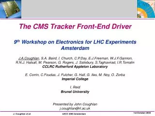
This document outlines the agenda for the interim review of the CMS Tracker FED project, including project status, manufacturing issues, testing experiences, and future plans.

E N D
Agenda • Agenda • Morning 08:30 -> 12:00 (Refreshments are booked for 10:00) • 1. Introduction. (60 minutes) • Overview Project Status and Future Plans. John • Feedback. All • 2. Board Status • Brief review of existing Problem reports. All • 3. Manufacturing Issues • PCB and Assembly Quality. • Design tools, file formats etc.. • 4. Testing experiences. • JTAG etc Ivan, James • Crates, Equipment. • 5. Next Pre-Production FEDv2 • Changes relevant to FED from CALICE design. James • Other potential changes. James et al. • 6. AoB • ==== > Lunch at 12:00 • Afternoon 14:00 -> 16:00 • 1. Firmware Status. • 2. Future Firmware. • 3. Related issues, design tools , CVS etc.. • -------------------------------------------------------------------------
CMS Tracker ReadoutOverview Task: To readout a very large Silicon Tracking detector. ~ 9 million Silicon Strip channels ON Detector: 73K APV25 pipeline chips @ L1 Trigger: MUX APV Frame output Analogue Data readout via Optical links (APV Frame: Header + Strip Data) => INS Effort : essentially complete OFF Detector: Front-End Drivers (FED) Digitise / Zero Suppress / DAQ readout ~ 500 x 9U VME64x boards (incl spares) 96 ADC channel boards => INS Effort : major activity 25 Front-End Hybrid Hybrid Silicon Strips 70m On Detector (Hard Radiation) FPGA DAQ Counting Room VME 9U FEDs
CMS Tracker FED INS Main Deliverables (Project Spec) • RAL INS • RAL PPD • Imperial College • Brunel FED project institutes: • Includes • Design of 9U FEDs. Electrical tests of design. • Design & Testing Baseline FPGA Firmware. • Production of prototypes for CMS silicon tests. • Production and Testing of ~ 500 FEDs (incl spares.) • Transition cards for DAQ links (tbd) • Low level driver software. • Full Documentation. • Communication with CMS groups • Assistance during Tracker installation & commissioning. • Excludes • OptoRx design & testing. • Opto Test equipment for FEDs. • DAQ link mezzanine card. • High level software. • Provision of VME crates and cabling. • Other modules in FED VME crates e.g. CPUs.
CMS Tracker FED Schedule Production & Installation NOW-> Design Test Pre-Pro FEDv1 FEDv2 FEDv3 • Tracker/FED installation schedule delayed by ~ 6 months wrt old CMS plan. • FED production & installation now expected in 2005 • Pre-installation lab area at CERN ready beginning 2004
CMS Tracker FED INS Dept Outline Tasks • FY 02/03 • Manufacture 2 x FEDv1. • Complete VME Firmware (EF) [4 months] • Complete BE Firmware (ST) [4 months] • Basic board tests Power/JTAG/Analogue (JS, IC) [3 months] • Primitive Driver Software (JC) [4 months] • FY 03/04 • Test of FEDv1 Design: (by Designers) • Advanced board tests (Opto tests @ IC) (IC, ST) [6 months] • Firmware (Front End & Event readout) (EF, ST) [6 months] • VME Interface (EF) [6 months] • DAQ interfaces (with Imperial) (ST, JC) [6 months] • Transition board (ST) [3 months] • Driver Software (JC) [6 months] • Production of 20 FEDv1s for CMS tracker testing. (IC, ST, JC) [6 months] • FY 04/05 • Pre-Production and Test of 20 x FEDv2. (ST,IC,JC) [12 months] • Procurement for 500 FEDs. (JC) [9 months] • Set up for “automated” Production Tests. (IC,ST,JC) [12 months] • FY 05/06 • Manufacture of 500 x FEDv3. (ST,JC) [12 months] • Production Testing @ RAL (IC +) [12 + months] • Assist Installation & Commissioning @ CMS. (JC,ST) [6 months] • FY 06/07 • Complete commissioning @ CMS. (JC,ST) [9 months] • Operation
CMS Tracker FED INS Dept Effort Design Test Production & Installation Includes APV effort ~ 2 SY integrated • Approx. 6 months behind original FED schedule. (but Tracker installation is also delayed). • Spent more time and effort getting design of FEDv1 close as possible to Production requirements. • (OptoRx and DAQ link specifications came later than expected). • Gross manpower figures are still reasonable. But no slack. • Profile needs adjustment.
12 12 12 12 12 12 12 12 CMS Tracker FED Block Diagram 96 Tracker Opto Fibres CERN Opto- Rx Modularity 9U VME64x Form Factor Modularity matches Opto Links Data suppression board. 8 x Front-End “modules” OptoRx/Digitisation/Cluster Finding Back-Endmodule / Event Builder VME module / Configuration Power module Other Interfaces: TTC : Clk / L1 / BX DAQ : Fast Readout Link VME : Control & Monitoring JTAG : Test & Configuration 9U VME64x Analogue/Digital JTAG FE-FPGA Cluster Finder FPGA Configuration VME Interface VME-FPGA BE-FPGA Event Builder TTC TTCrx DAQ Interface Buffers Power DC-DC Temp Monitor Front-End Modules x 8 Double-sided board Xilinx Virtex-II FPGA
CMS Tracker FED Firmware Status 22nd August 2003 System ACE EPROM VME FPGA Ed DAC Opto Rx EPROM Temp ADC System ACE DAC Opto Rx VME Bus Temp ADC Temp VME I2C Clocks Serial Comms Regs Clocks Serial Comms Regs Input Serial Comms VME LINK Data Data Header Mode Header Mode Cluster Mode Input Ed FIFOs DELAY FPGA x 3 x 8 Scope Mode Output BE FPGA Saeed Scope Mode Serial Comms Regs VME Link External Devices FE FPGA x 8 Ivan To be Implemented Control S-LINK S-LINK Clocks Headers Under Simulation Throttle TCS Input Under Test on FED QDR Write QDR Read TTC chanA TTCrx Data Readout Saeed, Ivan “Working” on FED Chan B QDRs Controls Ed, John FEDv2
FEDv1 Front-End module Primary Routed OptoRx OpAmps ADCs 40K FPGAs 1500K FPGA Dense circuitry Note: FPGA de-coupling 12 optical channels
12 12 12 12 12 12 12 12 CMS Tracker FED Transition card option Due to mechanical constraints place DAQ link card on Transition card Transition Card Very simple card BE-FPGA Event Builder DAQ Mezzanine Card TTC TTCrx S-LINK64 DAQ Front-end Readout Link FRL Buffers
40 K ADC Channels 10 Bit@40MHz Max Trigger Rate 100 kHz Input Rate 1.5 T Byte/s Output rate 25 Gbyte/s/% CMS Tracker FED Crate Layout (illustration) FED DAQ • 440 Boards 96 ADC/Board • 24 Crates • 8 Racks 4 TTC Partitions