Download
1 / 28
280 likes | 308 Views
STAR upgrades: New TPC FEEs Micro-Vertex Detector. DOE Review Jan 2004 Howard Wieman. STAR TPC FEE upgrade. Replace current STAR TPC FEE and RDO with ALICE components Tech transfer from CERN (went the other way for NA49) Lead Engineer: Fred Bieser.

E N D
STAR upgrades: New TPC FEEs Micro-Vertex Detector DOE Review Jan 2004 Howard Wieman
STAR TPC FEE upgrade • Replace current STAR TPC FEE and RDO with ALICE components • Tech transfer from CERN (went the other way for NA49) • Lead Engineer: Fred Bieser
ALICE PASA and ALTRO chips What they will do • Higher Event Rate to Level 3 (>1KHz) • X10 improvement • 20MHz/10bit ADC per channel (4mW) • Continuous Waveform Sampling • Digital filtering (better shaping) • Tunable pulse shaping (tail corrections) • Zero suppression before Xmission to DAQ • More room available for other detectors preamp shaper digitize adj. baseline suppress 0s serialize send to DAQ
STAR FEE/RDO Design Status • New FEE designed • New FEE ½ size of old (but no space gain) • Will use same cooling and mounting structure • Twisted pair cable will couple to new Read Out Board • RDO • Replacement will free up 4 in between TPC and Calorimeter • Again will use the existing support and cooling • RCU (collector to optical fiber) Standard CERN protocol • Test chips at LBNL
What physics? Charm quark yield measuring Ds Measure c quark yield in p-p and Au-Au collisions Normalize J/Y production rate B Mesons High statistics to understand c dynamics -final state parton interactions (partonic flow) vs initial state parton interactions High statistics to understand flavor chemistry Measurement including mVertex is 100 X faster than TPC+SVT+TOF alone Micro Vertex for precision heavy flavor measurements
Micro Vertex design issues • Must be very thin • Driven by multiple scattering in a high multiplicity environment • Must be air cooled (consequence: limited power budget) • Thinned silicon 50 m • Excellent two hit resolution • High track density • 30 m by 30 m pixels • 100 Mega Pixels • Can be relatively slow initially for X4 RHIC design luminosity • First generation with nearly current Monolithic Active Pixel Sensor (MAPS) technology • Upgraded luminosity requires faster readout • second generation MAPS with on chip 0 suppression • Replacement silicon costs: 215k$ - 360k$ • Mechanics design for easy insertion and extraction – upgrade replacement and ease of maintenance • Single end support allows installation with preserved measured alignment
Commitments • LBNL - LDRD funds FY 2002 – 2004 375k$ • Relativistic Nuclear Collisions Group • Howard Wieman • Hans-Georg Ritter (RNC Group Leader) • Fred Bieser (Lead Electronic Engineer) • Howard Matis • Leo Greiner • Fabrice Retiere • Eugene Yamamoto • Kai Schweda • Markus Oldenburg • Robin Gareus (Univ. Heidelberg) • LEPSI/IReS (Strasbourg) • Claude Colledani, Michel Pellicioli, Christian Olivetto, Christine Hu, Grzegorz Deptuch Jerome Baudot, Fouad Rami, Wojciech Dulinski, Marc Winter • LBNL Mechanical Engineering • Eric Anderssen (consultation – ATLAS Pixels) • Design works • UCI • Stuart Kleinfelder + students • BNL Instrumentation Div (consulting) • OSU • Ivan Kotov • Purdue • Dennis Reichhold
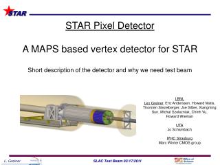
STAR Micro Vertex Detector • Two layers • 1.5 cm radius • 4 cm radius • 24 ladders • 2 cm X 20 cm each • < 0.2% X0 • ~ 100 Mega Pixels
Micro Vertex topics • 1st generation detector using Monolithic Active Pixel Sensors (MAPS) from LEPSI/IReS Strasburg • Readout concepts - LBNL • “Piggy Back” Custom chip • Off ladder digitization • R&D program for 2nd generation silicon • Mechanical development • CMOS schedule and cost
MIMOSTAR LEPSI/IReS for first generation STAR detector • Based on MIMOSA-5, full wafer engineering run – significant readout infrastructure on chip • LBNL test board works (Bieser and Gareus) • 2 by 2 cm MIMOSA-5 chip • LBNL development using 4 commercial 50 MHz 14 bit ADCs • MIMOSTAR Design • 1.9cmX1.9cm active • 30mX 30m pixels 409600 pixels/chip • Continuous frame read at 4-8ms per frame • 52 mW per chip • Analogue readout options • Single fast option 50 to100 MHz • 10 at 10 MHz option
Readout Options • Analogue cabled to ADC boards with memory and signal processing and zero suppression • Limits on speed and ladder size, i.e. room on cable for traces • Fred Bieser design • Or Piggy back readout out chip for same purpose • 10 ADCs working in parallel • Much less data to move off the ladder (0.5%) • Thesis project, Robin Gareus (Univ. Heidelberg at LBNL)
Advanced APS designs for generation 2 • Goal, increase speed with on detector chip zero suppress and by avoiding full frame readout • Requires improvements in signal to noise • Noise sources • KTC reset noise • Fixed pattern noise, threshold variation, leakage current variation • Programs at LEPSI/IReS • Programs at UCI/LBNL (Stuart Kleinfelder, Yandong Chen) • Photogates • CDS clamp circuit • Active Reset
Photo gate purpose - addresses standard diode limitations Standard APS diode structure • Correlated Double Sample on chip • Improved charge collection P P- P+ Standard diode geometry
Photo-gate geometry • Large photo gate area for collection • Transfer to small capacitance node photo gate transfer gate drain photo gate 20 m
Mechanical • Rapid insertion and removal • Rapid replacement - insurance for beam excursion damage • Minimum thickness: 50 Micron Si Detector – 50 Micron Si Readout chip • Air cooling • Composite beam pipe?
Inner vertex detector in STAR New vertex detector centered in existing SVT, supported one end only End view showing 3 of 6 ladder modules
aluminum kapton cable (100 m) silicon chips (50 m) 21.6 mm 254 mm carbon composite (75 m) Young’s modulus 3-4 times steel Thin stiff ladder concept • Under development • Will be tested for vibration in our wind tunnel
Thin silicon ladder, tension support Lucite wind tunnel Laser light source Camera TV Holography from ATLAS, LBNL
MAPS Silicon Schedule (LEPSI/IReS) Detector installation 2008
Summary • Design work progressing on STAR TPC FEE/RDO replacement with ALICE design • Design work progressing on MAPS by LEPSI/IReS (the 1st generation sensor for STAR inner vertex • Developing Readout approaches • R&D for 2nd generation sensors by UCI/LBNL • R&D mechanical concepts for detector support system • Installation in 2008
50 m Silicon Thinned Silicon wire bonded to cable, both supported under tension Thinned and polished wafers, a standard industrial process “Wind tunnel” tests in preparation for testing cooling and vibration stability
Silicon Cost 8 inch wafers 20 mm x 170 mm ladders