Download
1 / 35
370 likes | 661 Views
VLSI Design Lecture 4-a: Layout Extraction. Mohammad Arjomand CE Department Sharif Univ. of Tech. Adapted with modifications from Harris’s lecture notes. Topics. SCMOS scalable design rules. Reliability. Stick diagrams. MOSIS SCMOS design rules.

E N D
VLSI DesignLecture 4-a: Layout Extraction Mohammad Arjomand CE Department Sharif Univ. of Tech. Adapted with modifications from Harris’s lecture notes
Topics • SCMOS scalable design rules. • Reliability. • Stick diagrams.
MOSIS SCMOS design rules • Designed to scale across a wide range of technologies. • Designed to support multiple vendors. • Designed for educational use. • Ergo, fairly conservative.
and design rules • is the size of a minimum feature. • Specifying particularizes the scalable rules. • Parasitics are generally not specified in units
Wires metal 3 6 metal 2 3 metal 1 3 pdiff/ndiff 3 poly 2
Transistors 2 2 3 3 1 5
Vias • Types of via: metal1/diff, metal1/poly, metal1/metal2. 4 4 1 2
Metal 3 via • Type: metal3/metal2. • Rules: • cut: 3 x 3 • overlap by metal2: 1 • minimum spacing: 3 • minimum spacing to via1: 2
Tub tie 4 1
Spacings • Diffusion/diffusion: 3 • Poly/poly: 2 • Poly/diffusion: 1 • Via/via: 2 • Metal1/metal1: 3 • Metal2/metal2: 4 • Metal3/metal3: 4
Overglass • Cut in passivation layer. • Minimum bonding pad: 100 m. • Pad overlap of glass opening: 6 • Minimum pad spacing to unrelated metal2/3: 30 • Minimum pad spacing to unrelated metal1, poly, active: 15
Lithography for nanometer processes • Interference causes drawn features to be distorted during lithography. • Optical proximity correction pre-distorts masks so they create the proper features during lithography.
3-D integration • 3-D technology stacks multiple levels of transistors and interconnect. • Through-silicon-via (TSV) with die stacking uses special via to connect between separately fabricated chips. • Multilayer buried structures build several layers of devices on a substrate.
Reliability • Failures happen early, late in chip’s life. • Infant mortality is caused by marginal components. • Late failures are caused by wear-out (metal migration, thermal, etc.).
Mean-time-to-failure • MTF for metal wires = time required for 50% of wires to fail. • Depends on current density: • proportional to j-n e Q/kT • j is current density • n is constant between 1 and 3 • Q is diffusion activation energy • Can determine lifetime from MTTF.
Traditional sources of unreliability • Diffusions and junctions: crystal defects, impurity precipitation, mask misalignment, surface contamination. • Oxides: Mobile ions, pinholes, interface states, hot carriers, time-dependent dielectric breakdown. • Metalization: scratches/voids, mechanical damage, non-ohmic contacts, step coverage.
TDDB • Time-dependent dielectric breakdown: gate voltages cause stress in gate oxides. • More common as oxides become thinner. • TDDB failure rate: • MTTF = A 10 bE eEs/kt
Hot carriers • Hot carrier has enough energy to jump from silicon to oxide. • Accumulated hot carriers create a space charge that affects threshold voltage.
NTBI • Negative bias temperature instability is particular to pMOS devices. • Threshold voltage, transconductance change due to stresses. • Can be reversed by applying a reverse bias to the transistor.
Electromigration and stress migration • Degenerative failure for wires. • Grains in metal have defects at grain surface that cause electromigration. • Stress migration caused by mechanical stress. • Can occur even with zero current.
Soft errors • Caused by alpha particles. • Packages contain small amounts of uranium and thorium, which generate error-inducing radiation.
PVT • Borkar et al.: variations in process, supply voltage, temperature are key design challenges in nanometer technology.
PVT challenges • Process variations: channel length and threshold significantly in nanometer technologies. • Supply voltage: non-ideal wires introduce variations in supply across chip. • Temperature: higher chip operating temperatures degrade both transistors and interconnect.
On-chip temperature sensors • Temperature sensors are used to shut off part or all of the chip to stop thermal runaway. • Use a pn junction from a parasitic bipolar transistor. • Can also use MOS transistor.
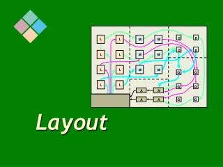
Stick diagrams • A stick diagram is a cartoon of a layout. • Does show all components/vias (except possibly tub ties), relative placement. • Does not show exact placement, transistor sizes, wire lengths, wire widths, tub boundaries.
Stick layers metal 3 metal 2 metal 1 poly ndiff pdiff
Dynamic latch stick diagram VDD in out VSS phi phi’
Sticks design of multiplexer • Start with NAND gate:
NAND sticks VDD a out b VSS
One-bit mux sticks VDD N1 (NAND) N1 (NAND) N1 (NAND) ai bi a a a out out out select’ select b b b VSS
3-bit mux sticks select’ select m2(one-bit-mux) select’ select VDD ai a2 oi o2 bi VSS b2 m2(one-bit-mux) select’ select VDD a1 ai oi o1 b1 bi VSS m2(one-bit-mux) select’ select VDD a0 ai oi o0 b0 bi VSS
Layout design and analysis tools • Layout editors are interactive tools. • Design rule checkers are generally batch---identify DRC errors on the layout. • Circuit extractors extract the netlist from the layout. • Connectivity verification systems (CVS) compare extracted and original netlists.
Automatic layout • Cell generators (macrocell generators) create optimized layouts for ALUs, etc. • Standard cell/sea-of-gates layout creates layout from predesigned cells + custom routing. • Sea-of-gates allows routing over the cell.
Standard cell layout routing area routing area routing area routing area