Download
1 / 43
470 likes | 760 Views
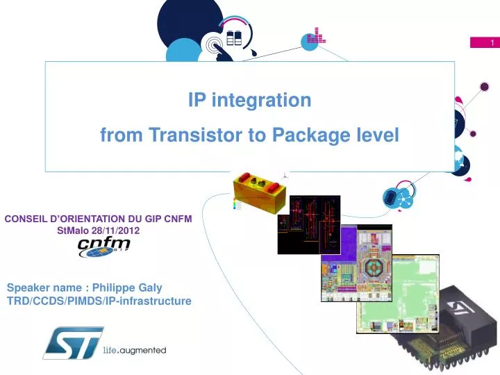
IP integration from Transistor to Package level. Speaker name : Philippe Galy TRD/CCDS/PIMDS/IP-infrastructure. CONSEIL D’ORIENTATION DU GIP CNFM StMalo 28/11/2012. Outline. Integration context Focus on ESD : Events to IP solution Package & 3D connections

E N D
IP integrationfrom Transistor to Package level Speaker name : Philippe Galy TRD/CCDS/PIMDS/IP-infrastructure CONSEIL D’ORIENTATION DU GIP CNFM StMalo 28/11/2012
Outline • Integration context • Focus on ESD : Events to IP solution • Package & 3D connections • Tooling : Checkers & Builders • Partners & collaborations
Integration context • Focus on ESD : Events to IP solution • Package & 3D connections • Tooling : Checkers & Builders • Partners & collaborations
Context IP integration question of scale factor • IP or Macro IP is a complex design • Integration need to be compliant to package level 4
Context • Complex Process flow • Complex facilities • Etching ; Plasma, RIE , Implantation … • Flavors of substrate : Bulk or PD/FD SOI 200 – 300 mm Wafer Human Machine
gate gate Thin Silicon film Silicon Substrate Technology context : FEOL Context • Thin & Thick oxide gate transistor • High K metal gate • Different topologies ; sub nanometer • Scale down of transistors & metal layers • Flavors of substrate : Bulk or PD/FD SOI Gordon Moore Planar MOSFETs Bulk FD SOI 20 nm 14 nm 10 nm and beyond
Technology context : BEOL Context • Stack metal : M1 to M11 • Low K inter dielectric • Complex Stack & Via structure Sub-Nano MOS transistor (FEOL) Gate stack Metal Stack (BEOL)
IP context Context High Density Memory • Dig/ ANA/ RF IP • LOW leakage IP • GO1/GO2 IP transistors • Multi Applications • 1 000 000 000 XTors High Density Blocks Complex IO ring SOC view
1000 500 200 Apps 100 FEnd PMIC Network 50 90/80 nm 2004-2007 65/55 nm 2005-2010 45/40 nm 2008-2011 32/28nm 2009-2014 20nm 2012-20xx SOC context Context 10 CPU/GPU’s, >2GHz, ~3-7W, Flip Chip / 3Dstack Heterogeneous Mtr • Dig/ ANA/ RF SOC • LOW power / FAST SOC • Multi processor • Multi Applications • 1 000 000 Trs 8 CPU/GPU’s, 1-2GHz, ~3-7W, FC, system on single package 6 CPU/GPU’s, 700MHz, ~3-6W, WB, Flip-Chip, System Co-design 5 CPU’s, 500MHz ~3-4W, WB, FE integration 3CPU’s, 250MHz, ~3W, Hierarchical Design, Wire bonding Leader • 28nm FDSOI Available • - 24 nm possible • - Back Bias • Poly Bias • - Co integration (Bulk + FD SOI) 9
Package context Context • Dig/ ANA/ RF • Multi Dice • Multi connections • Thermal behavior Design/SOC Assembly Final Package Backside view
System context Context • Dig/ ANA/ RF SOC • Power management • Multi Applications • Multi Chips • Multi protocol • Multi standard • Multi environment • Robust solution • Full Plat-Form solution
Integration context • Focus on ESD : Events to IP solution • Package & 3D connections • Tooling : Checkers & Builders • Partners & collaborations
A 30 HBM IEC 8kV contact 20 CDM 500V 15 10 t ns 5 HBM 4 kv 0 0 20 40 60 80 100 120 MM 200V ESD event : True life • At least four standards are used to qualify a solution • Human Body Model (HBM) • Machine Model (MM) • Charged Device Model (CDM) • Human Metallic Model (HMM or Gun) • Different energy stresses: 1A, 2A & 30A • Different stress durations: 1ns to 100ns • Comparison • HBM, CDM, CDM & IEC Stress
ESD Challenges ESD context • Different energy stresses: 1A, 2A & 30A • Different stress duration: 1ns to 100ns • One or Two pins stressed • Can occurs all along the chip lifetime Chip context • Digital/Analog/RF and multi powers/Dice • Thin & Thick oxide gate transistor • Scale down of transistors/metal layers • Low power / Fast signal • Multi balls (1000) / multi dice/huge die size (100mm2) • Flavors of substrate : Bulk or PD/FD SOI ESD Co-design Challenge • Provide efficient power devices • Provide efficient trigger circuit • Optimize : Silicon area, leakage, parasitic capacitance • Address all ESD standards for all IPs/Ios (RF/ANA/Dig) • Develop Robust & reliable ESD strategy for SOC (IO+core) • Take into account process discrepancy ESD Tools/Checkers Challenge • Checker for IP/IO & core IPs • Pertinent /Robust/portable checkers Perform a Robust Design thanks to checkers CCDS 10 000 000 instances & more 14
Device Solutions • Different devices are required to address this challenge • Power device as primary protection • Fast device as secondary protection • Standard device as trigger element • Advanced device as new solution • Optimize silicon area • Optimize signal integrity • Don’t forget robust Metal & Via connection • (not discussed here)
Device Solutions • Example : BIMOS transistor • BIMOS Tr = Bipolar + MOS Effects (Theoritical view) • Design solution to catch : • Dynamic ESD event • Quasi Static ESD event Single BIMOS TC • Dynamic Response R • Quasi-static Response Zener ! (Body + gate bias)
Example : Triac power device Device Solutions Basic schematics • Classic Equations (*) Equation de Poisson (*) Equation de continuité (*) Equation de transport • (*) Equation de la chaleur A1 A1 Gate N Gate N SCR#2 SCR#1 A2 A2
Device Solution • Example : Beta Matrix Matrix Sub Matrix Cross Section 1.5 Power device Concept Extraction point 1 A2 A1 0.5 A2 Pw 3D TCAD Pw Pw Pw Pw Pw Pw Pw Pw Pw Isotherm IV response Current density extraction 0 N+ P+ P P P P P P P P P N N N N N N N N N N+ P+ 2 3D TCAD results 0 4 8 6 10 Current (A) Pwell Pwell Pwell N+ N N N N N N N N N P+ P P P P P P P P P N+ N+ P+ P+ Nwell Voltage (V)
Device Solution • Example : Beta Matrix & HC Equations set 3D TCAD study FA “Hot” Zoom In Cross section
Trigger Solution • Trigger Circuit : • Dynamic detection event in the ESD range time • Static detection event through threshold • Both detection • Optimize silicon area • Fast response • Low energy behavior • Designed for the ESD window
ESD IP Solution • R&D differentiation : Before & After IP integration 2 IOs pitch MOSSWI +DIODE Mosswi MOSSWI+ diode R C After Before 1 IO pitch Bi-SCR R SCR + SCR C SCR SCR After Before
Clamp VDD2 TC TC TC TC TC TC TC TC ESD IP Solution • Example : HBM+MM+CDM+HMM • Power device + Dynamic Trigger • Modular approach P1 R D1 Dual SCR Elementary Module Silicon measurements VDD1 VDD2 Clamp IO IO IO P2 IO R VDD1 VSS1 VSS2 New ESD network
ESD Gun ESD protection strategy ESD GUN context • Energy stress: 30A at least • Stress duration: 1ns rise time to 100ns • Two pins stressed contact or air discharge • Power off & Power on • Standard : IEC 61000-4-2 Board/ Chip context • Digital/Analog/RF and multi powers/Dice • Thin & Thick oxide gate transistor • Multi chips / multi dice / multi balls • Flavors of substrate : Bulk or PD/FD SOI • External connectors/ PCB routing ESD Gun Co-design Challenge • Provide efficient power devices • Provide fast trigger circuit • Optimize : Silicon area, • leakage, • parasitic capacitance • Address all ESD standards (HBM/MM/CDM) • Avoid LU Solution reaches 30A target ! 23
ESD CDM Current [A] Time [sec] Kelvin Pad frame for VFLTP & VF TCS ESD protection strategy 2 1 4 3 Development of tools devoted for CDM study Evaluation of protectiondevices in time range of CDM Evaluation of full CDM protection strategy on IO Development of package model Identification of the main phenomenon involved during stress Static CDM check on IP Dynamic CDM Check on IP block Ground plate RTEST1W CPM LTEST RARC VCDM CDut RCHRG 1GW Field plate Basic schematic of the problem to simulate • Pogo pin contribution • Package contribution • Metal contribution • Design contribution • Layout contribution • Substrate contribution
ESD CDM ESD protection strategy Macro IP R&D collaboration Global view of extractions & activities . Link with TDDB Extract #1 @ 6 ps Extract #3 @ 326 ps Extract #2 @ 249 ps Extract #4 @ 512 ps
Tong effect = Hole + partial Snapback CDM silicon signatures • CDM silicon signatures & physical phenomenon : • Typical CDM silicon signatures identified • Physical mechanism : Snapback and/or dielectric breakdown • Examples of signatures see below Backside view Snapback Filament (hard fail) Hole in gate Drain side Snapback Hole in gate (Soft fail) Multi Holes in gate Failure Analysis Item & associated expertises Substrate current 19-Sep-14
FOCUS ESD RF & Beyond ! Ref : Dimitri Liten ICICDT 2010 Our target Best Solution Local clamp STM C65 SCR+Diode (15µm x 15µm) 30 GHz 400 MHz • How to reach the ESD/RF targets • 2KV HBM for 20 GHz bandwidth at least
ESD RF & Beyond ! Aν = (φ,A), Jν = (ρ,J) Quadri vectors : R&D collaboration ∂ν Aν = 0 Lorenz gauge : Maxwell Faraday tensor : Fµν = ∂µAν - ∂νAµ ∂µ Fµν = - 4п Jν Maxwell equation: Vectors : E = -∇φ - ∂t A , B = ∇×A Silicon Transport equations : Jn = q μn n (E + vn × B) + k T μn∇.n Coupled with Lorenz force Jp = q μp p (E + vp × B) – k T μp∇. p Continuity equation : ∇· J = - ∂t ρ + U Metal Transport equation : J = σ.E + μHJ × B Coupled with Lorenz force
ESD RF & Beyond : Minimize parasitic Capa FEOL + BEOL parasitic capacitance calculation thanks to coupled equations for local clamp solution BEOL Bandwith calculation FEOL+BEOL extraction FEOL+ BEOL capacitance = 80 fF FEOL It’s possible to extract E, B fields into the structure (@10GHz) E(V/m)
ESD RF & Beyond ! Our target Best Solution Local clamp STM C65 SCR+Diode (15µm x 15µm) New target 30 GHz C40,32 demonstrators 400 MHz How do to ?
Beyond : Embedded protection in propagation line Topology E distribution Hdistribution Jn distribuition in Si substrate Model Measure RF Measurements 100GHz OK
R&D collaboration Metal behavior • Full 3D ESD device • Current density Time Evolution
Integration context • Focus on ESD : Events to IP solution • Package & 3D connections • Tooling : Checkers & Builders • Partners & collaborations
Package & 3D connection • Complexity of package increases with technology node ! • Several layers, material … • SOC, SIP …. Pin number 1500 pins QFP (Quad Flat Package) 1 000 pins QFN (Quad Flat No-leads) 500 pins 200pins BGA (Ball Grid Array) SOP (Small Outline Package) 64pins 48pins PGA (Pin Grid Array) 16pins DIL (Dual In Line) 34
SIP 3D interconnect • Example of contribution on signal Integrity • Cu pillar, Ball , TSV 3D interconnect • Multi substrate package layers • Interposer ….. 32 nm stacked on 65 nm Die TSV TSV 40GHz 35
Transient domain • DDR application • To include BDPROG IO spice netlist • Load => Memory + Memory Package (POP configuration) • Bump RDL impact Bump to RDL impact X pF TL model IO:BDPROGMOBLPDDRSCARUDQP_URISO_SF_1V2_DQ_FC_LIN_PHY Zout=34Ω ASRCN<6:0> = 0101000 ASRCP<6:0> = 1010101 Spectre models – Typical corners output_package input W,L Package (SDRDQ2) Vs IO Spice Netlist MSub Freq = 500MHz Vhigh = 1V
Integration context • Focus on ESD : Events to IP solution • Package & 3D connections • Tooling : Checkers & Builders • Partners & collaborations
IP integration with Flexframe Tool Integration • Design & topology for example ESD IP • Flex frame integration and generator tool gnde ESD Design … Final Delivery IP IO Offer LB IO pin IPs (schematic + block layout) ANA Mtop IO pin DIG Synchronicity SUPPLY vdde STAND. gnde Special Flexframes Others … esdsub esdsub
CAD/TOPO/EC Checkers Tool Check before/after IP development • Database environment setup • Topologic checks : DFM … • Electric checks : PISI/ESD/ERC/Aging … • Reports & waivers file Macro level Nano level
I/O ring builder/checkerTool Engines IO Builder/Checker during development • Builder/checker IO focused • Multi engines & thread • Data Model IP level • Provide optimized robust solution Checker Checker Data model Checker Technology Package Builder Builder Builder Library Library Library I/O list Power domains • Proposed Solution PLL example Area: 0.62 mm² Area: 0.21 mm²
Integration context • Focus on ESD : Events to IP solution • Package & 3D connections • Tooling : Checkers & Builders • Partners & collaborations
Partners & collaborations R&D collaborations • Universities & Laboratories • Thesis (open positions ) • Internships • Projects development • CAD Providers • National & European projects • Consortium
Thank You • Have a Nice Day • Do not hesitate to contact us