Download
1 / 40
410 likes | 676 Views
Multi-layered graphene and Graphene-like ultra THIN FILMS in MICROWAVES P. Kuzhir , K. Batrakov , A. Paddubskaya , S. Voronovich , N. Valynets , S. Maksimenko , Research Institute of Nuclear Problems of BSU , Belarus T. Kaplas and Yu. Svirko

E N D
Multi-layered graphene and Graphene-likeultra THIN FILMS in MICROWAVES P. Kuzhir, K. Batrakov, A. Paddubskaya, S. Voronovich, N. Valynets, S. Maksimenko, Research Institute of Nuclear Problems of BSU, Belarus T. Kaplas and Yu. Svirko University of Eastern Finland, Finland
Investigated films: • Pyrolytic carbon (PyC), 5-240 nm thick • A few-layer graphene, 5 nm thick (10 layers) • Sandwich structure: graphenemonolayers + PMMA • All investigated films are deposited on 0.5 mm thick silica substrates • Synthesis • Characterization • Microwave probing (Ka-band, 26-37 GHz) • Comparative analysis of EMI SE provided by ultra-thin films and conventional polymer composites filled with nanocarbon, and carbon foam
MICROWAVE PROBING of GRAPHENE-LIKE ultra THIN FILMS: challenge Film thickness PyC = 5-240 nm Film thickness multilayered graphene = 5 nm (10 layers) Film thickness of sandwich structures = 2 or 3 graphene monolayer + PMMA (600-800 nm) skin depth in microwave range = tens of microns (15-20 microns) Film thickness skin depth graphene-like ultrathin films should be transparent for microwaves ? http://www.microwaves101.com/encyclopedia/skindepth.cfm
Pyrolitic Carbon thin films: methane-based chemical vapor deposition • We employed CVD process with no continuous gas flow inside the chamber to reduce gas consumption and to allow more time for polyaromatic structures formation. • The loading of the clean quartz substrate into the CVD chamber was followed by purge filling of the chamber with nitrogen (twice) and then with hydrogen to ensure a clean process. • After that the chamber was filled with hydrogen up to the pressure of 5.5 mBar and was heated up to the temperature of 700 °C at the rate of 10 °C/min. • At 700 °C, the chamber was pumped down and the hydrogen-methane gas mixture was injected and heated up to the temperature of 1100 °C. • CH4:H2 gas mixture was kept at this temperature for 5 min and then was cooled down to 700 °C. After that the chamber was pumped down, filled with hydrogen at the pressure of 10 mBar and cooled down to room temperature.
Parameters of the synthesized PyC films Thickness of prepared carbon films was measured by a stylus profiler (Veeco Instruments, Dektak 150) with an accuracy of 1.5 nm. • The thickness of deposited film is dependent on methane concentration. • Ultrathin PyC films of prescribed thickness in the range of 5-240 nm were synthesized.
Raman characterization perfect graphite “G” peak ”D” (disorder) peak • Raman spectra of the manufactured PyC films by using Renishaw inVia Raman Microscope at the excitation wavelength of 514 nm. • The Raman spectrum of perfect graphite dominates by “G” (graphite) peak, 1582 cm-1 and indicates the presence of the crystalline graphite in the sample. • The disorder broadens the G-peak and usually results in ”D” (disorder) peak in the vicinity of 1360 cm-1. • The ratio of these peaks I(D)/I(G)is conventionally used as a measure of graphite crystallinity. In an ideal graphite, I(D)/I(G) = 0, while in highly disoriented PyC, this ratio is relatively high, I(D)/I(G) ≥1.
Raman characterization the ratio of the sp2-sp3 bonds graphitic lattice defects amount of amorphous carbon • In the thinnest films, I(D)/I(G) = 1.2, while in the thickest films, I(D)/I(G) = 1.0. • Positions of D and G peaks were at 1357 cm-1 and 1595 cm-1, respectively, and did not depend on the film thickness. • The G-peak situated in the vicinity of 1600 cm-1 indicates that the film is mainly consists of sp2 bonded graphene nanocrystallites, i. e. its morphological properties are close to those of nanographite. • A finite magnitude of the D” peak suggests that the film contains also amorphous carbon. • Crystallinity of the film can be evaluated from the full width half maximum of the G-peak in the Raman spectrumFWHMG ≈ 70 cm-1 : the size of graphite crystallites is to be less than 5 nm.
Transmittance, optics Transmittance spectra was measured with Perkin Elmer Lambda 9 spectrophotometer in the spectral range from 200 nm to 2000 nm. The transmittance was measured with respect to a bare fused silica substrate. The transmittance is almost constant in the visual and IR spectral range having a minimum at wavelength of 270 nm. The obtained featureless transmission spectrum in visible spectral range is typical for graphitic materials (e.g. graphene). It ensures no significant coloring, i.e. the ultrathin carbon films are well suited for transparent conductive electrodes. Optical transmittance of the PyC films as a function of wavelength.
Sheet Resistance vs Optical Transmittance A V Sheet resistance versus optical transmittance is comparable to chemically derived graphene. Quartz • The sheet resistance Rs of the PyC films was measured with the conventional four-point probe technique. • The setup was based on probe station (Signatone S-1160) with 2 mm probe spacing and U = 5 V driving voltage. • Since the thickness of the samples was considerably less than the probe spacing, the sheet resistance can be obtained as:
Microwave probing in Ka-band (26-37.5 GHz) The EM response of samples as ratios of transmitted/input (S21) and reflected/input (S11) signals was measured within the 26-37 GHz frequency range (Ka-band). The waveguide cross-section was 7.2×3.4 mm. Ka-band (26-37,5 GHz) Scalar analyzer R2-408R(VSWR and Transmission Loss Meter R2-408R)
Microwave probing of PyC films 28 GHz • Reflectivity of PyC films of relatively small thicknesses (up to 28 nm) is almost the same as for bare quartz substrate (these films reflect 20-22 %). • Films with thickness higher than 30 nm reflect from 27 to 34 % of EM radiation. • In the PyC films with thickness lower than 75 nm, the absorption increases significantly with the thickness. • The thickest PyC films demonstrate significant EMI SE. Only 22, 18 and 16 % of microwave signal could penetrate through the PyC film with thickness of 75 nm, 110 nm and 241 nm, respectively, deposited on silica substrate. • Even 30 − 35 nm thick PyC films secure already about 60 % of EM attenuation at 28 GHz mostly due to absorption of the microwave radiation. Thus, fabricated PyC films, whose thickness is thousand times less than the skin depth of conventional metals, provide a reasonably high EM attenuation. Film thickness, nm
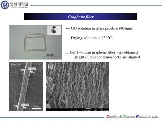
Multi-layered graphene films: catalytic CVD process • 0.5 mm quartz sample was coated with copper thin film which was physically deposited, i.e. by thermal evaporation in vacuum (10-5 mBar) condition, on the quartz surface. • The used copper layer thickness was 300 nm which is thick enough for surviving of dewetting in high temperature without making holes but thin enough for carbon atoms to get through grain boundaries. • Before the process, the CVD chamber was cleansed with nitrogen (twice) and hydrogen to remove oxygen remains from the chamber. • Next the Cu coated quartz sample was heated in hydrogen atmosphere (7 mBar) to 700 °C. • At this temperature hydrogen was pumped from the chamber and methane-hydrogen gas mixture (1:1) was injected in the chamber until the pressure was ~10 mBar. • The temperature was then risen to 950 °C with rate of 10 °C/min. • After 5 min the chamber was cooled down to 700 °C during 60 min and the CH4-H2 atmosphere was replaced with hydrogen (7 mBar). • After the CVD process, the remaining Cu was removed by ferric chloride (FeCl3) solution and rinsed with water.
Mechanism 25 °C ~700 °C ~1000 °C Silica substrate
Multi-layers graphene films: characterization For monolayer graphene the 2D peak position should be around 2680 cm-1 and the FWHM ~30 cm-1, while for multilayered graphene the 2D peak is shifted close to 2700 cm-1 and FWHM is increased up to ~60 cm-1. In our sample the 2D peak is located at ~2705 cm-1 and the FWHM is about 65 cm-1 indicating that the sample is a multilayered graphene rather than mono- or bi-layered graphene. Fig. 2. Atomic force microscopy image of graphene film. Fig. 1. Typical Raman spectrum measured from nanocarbon film indicates highly crystalline, multilayered graphene material.
Microwave probing of multilayered graphene films Fig . Reflection (R), transmission (T) and absorption (A) of graphene film vs frequency. In Ka-band we observed that multilayered graphene being thousands times thinner than skin depth of conventional metals provide reasonably high EM attenuation properties, caused by absorption of EM signal. EM absorption is as high as 43% at 26 GHz for graphene film of 5 nm thickness.
Sandwich structures: monolayer graphene + PMMA. Synthesis • The first graphene monolayer was synthesized by chemical vapor deposition (CVD) at 1000 C in methane atmosphere on the copper catalyst • and then spin coated by the 600-800 nm thick PMMA layer. • Next, Cu was wet etched in ferric chloride. • The obtained PMMA film with deposited graphene was washed in distilled water and then placed on quartz substrate. • After drying the next graphene layer was deposited on the top of the PMMA. • This procedure has allowed us to fabricate sandwich-like coatings containing two – three graphene layers.
Transfer and deposition of several graphene layers Spin coated PMMA Cu substrate Graphene Quartz
Sandwich structures: monolayer graphene + PMMA. Chatacterization The absorption of one layer on top of quartz should be about 1.9 - 2 %. Here are the results that we observed 1 layer 800.1827 0.9828 2 layers 801.0099 0.9521 3 layers 799.3555 0.9238 The absorption of 2 and 3 layers is a bit more than ~2 % but this is because that the “monolayer” is only about 90% monolayer. According to Raman spectrum investigations, monolayer graphene is 90-95% of monolayers and 10-5% of bilayer graphene.
Microwave probing of sandwich graphene+PMMA films • Graphene monolayer provide almost 20% of absorption of microwave signal at 28 GHz. • 2 layers of monolayered graphene separated by 600-800 nm of PMMA give 35 % of absorption of microwave power. • 3 layers provide almost 50% of MW absorption. • As far as neat PMMA is transparent to microwaves we suppose to have the same results for one-two and three monolayers of graphene (0.5 – 1.5 nm thick). • After removing PMMA, we will have 1.5-2 nm thick graphene films providing almost 50% of absorption of microwave power.
Conclusions. Graphene-like thin films in microwaves Graphene-like films being 100-1000 times thinner than skin depth provide reasonably high EM attenuation properties in microwave frequency range, caused by absorption mechanism. EM absorption is as high as 50% for PyC film of 75 nm thickness and multi-layered graphene, 1.5-2 nm thick. EM attenuation provided by PyC film of 30 nm thickness is compatible with EM attenuation of 1-2 wt.% commercial MWCNT embedded into epoxy, 1 mm thick The extremely small thickness and weight of graphene-like films makes them especially attractive for application in satellite and airplane communication systems. Moreover, PyC films and graphene films can be deposited on both dielectric and metal substrates of any shape or size by using conventional and inexpensive chemical vapor deposition technology. Thus, PyC and multi-layered graphene could be used as ultrathin, transparent, weightless, and flexible EMI shield, which would be tremendously important for portable electronic devices, transparent electronics and displays, and EM field isolation in 3D ICs.
High-frequency polarizability, microwave and THz range, modeling: Reasonable nanotubes parameters – 10-15 mkm length, 5-15 nm diameter, 7-10 walls. Length of nanotube is important both in MW and THz range Outer diameter of MWNT is important mostly in MW range Strong electromagnetic screening of inner shells take place in MW range (only 2-4 outer walls take part in EM interaction in MW frequencies). No electromagnetic screening takes place in THz range, all metal walls take part in EM interaction.
What should we expect from the theory of EM interaction of composite based on MWNT in • THz range (1-10 THz)? • No significant dependence on the mean outer diameter • Strong dependence on the length of CNT • No screening of inner shells of multiwalled CNT (all metal walls take part in EM interaction). • Therefore if we use CNT with as high number of walls as possible, they could be thin or thick, as long as possible, we could succeed with producing effective EM material for THz range application. • MW range (10-100 GHz)? • Some dependence on the mean outer diameter; • Strong dependence on the length of CNT • Quite strong screening of inner shells of multiwalled CNT (starting from 5th). • Therefore if we use CNT with small number of walls (up to 12-15), as thick and long as possible, we could succeed with producing effective EM material for MW range. • The number of walls as well as thickness of CNT can be controlled by catalyst and synthesis conditions. The optimal geometry of CNT to be used in MW and THz range could be different!
Microwave probing Ka-band (26-37,5 GHz): MWNT HR TEM micrographs (JEM-2010) of MWNTs samples with narrow distributions of average outer diameter (a–c), (d) the histogram of distribution of average outer diameter of these MWNTs. • MWNTs were synthesized by CVD methods via catalytic pyrolysis of ethylene at 950K on FeCo-based catalysts. • MWNTs were investigated with average outer diameter ~ 12-14 nm respectively. • The wall number has been estimated as 8-15 walls.
Materials used: Exfoliated graphite • EG was obtained by intercalation of natural graphite flakes, subsequently submitted to a thermal shock. • Accordion-like particles were produced, leading to a material of low packing density, around 3 g/L. • EG particles have the form of distorted accordion-like cylinders, having a typical diameter within the range 0.3 - 0.5 microns, and a aspect ratio around 20. Distorted honeycomb microstructure as seen by SEM. The constitutive graphite sheets may be seen as disoriented thin discs. Constituting individual worms of raw expanded graphite, as seen by SEM. A. Celzard, J.F. Marêché, G. Furdin, Progress in Materials Science 50 (2005) 93-179.
Microwave probing: Exfoliated graphite • High electromagnetic shielding efficiency in microwave frequency range has been found for epoxy/EG composites already for 1 wt.% of EG fillers. • When the concentration is below or equal to 1 wt.%, reflection of microwave signal is responsible for EMI shielding ability. 2 wt.% of EG within epoxy resin provides almost the same contribution of absorption and reflection mechanism into EM attenuation. • 2 wt.% EG in epoxy is not transparent to microwaves because of 45% of absorption and 55 % of reflection. S-parameters vs frequency for epoxy/EG composites with different contents of EG inclusions (0.25-2 wt.%). Inset: Transmittance (T), absorbance (A) and reflectance (R) provided by epoxy/EG at 30 GHz. One more advantage is that EG is easier dispersed in the epoxy resin.
Graphitic materials vs Carbon nanotubes Large surface area is extremely important
Dielectric permittivity of composite in range 20Hz – 1MHz The higher the structure (meaning that the CB comprises chain-like agglomerates, whereas less structured materials have more individual particles, not so much associated), the higher is the conductivity
30 GHz EG being embedded into epoxy in 2 wt.% is the best EM attenuator, but this concentration seems to be critical for mechanical properties
Carbon foams: Preparation carbon foams • Carbon foams are made of 95% of natural, green and renewable precursor. • Tannin is extract of acacia/mimosa bark. • Tannin is cross-linked with a little of formaldehyde in presence of furfuryl, ether and catalyst. • Carbonaceous counterpart is obtained by pyrolysis up to 900°C in high-purity nitrogen. • The density was simply adjusted from the amount of blowing agent (ether) in the initial formulation, the higher this amount, the lower the density and the higher the average cell size.
Carbon foams: Description, physical properties Skeletal density : 1.98 g/cm3 Bulk density : 0.025 – 0.20 g/cm3 Relative density : 1.3 – 10.1 % SEM images Porosity : 89.9 – 98.7 % 1 mm Estimated cost << 10 € / kg 500 µm Bulk density : 0.067 g/cm3 100 µm Main characteristics Average coordination number : 12 Porosity mainly open Bulk density : 0.067 g/cm3 compression strength = 0.25 – 2.25 MPa elastic modulus E = 0.7 – 35.5 MPa Electrical conductivity 1.5 – 40 S/cm thermal (k) conductivity k = 0.04 – 0.105 W/(mK)
Carbon foam: microwave range • EMI shielding efficiency has been found to be relatively high for 2 mm thick carbon foams, higher than 8 dB for samples with large pore size, the maximum at 23 dB EMI SE being obtained in Ka-band for the most dense samples. • The reflectance ability provided by studied foams characterized by the lowest density are not less than 7 dB in Ka-bands, which corresponds to approx 30 % reflection of incident signal. • Carbon foams with higher density reflect 75-50% of the microwave radiation.
Carbon foam: microwave range Reflectance (R), absorbance (A) and transmission (T) of the EM radiation on samples are connected with the measured S – parameters in the following way: R = S112, T = S212, A = 1 – R – T
Depending on properties and application field, different materials can be used Nano-Carbon based polymer composites Carbon foam • Could be produced in any shape, but finally rigid. • Fire resistant • Low cost • Light (7-25 times lighter than convetional polymers) • Manufacturability, processibility, • Thickness • Flexibility Ultra-thin carbonaceous films (PyC, graphene, etc) • Flexibility • Thickness • Weight • Corrosion resistance • Easy to produce (cheap CVD technology)