Download

1 / 27
270 likes | 427 Views
Center for Adaptive Optics 15 Nov 1999 Meeting . Microfabricated Segmented Micromirror Arrays. Major William D. Cowan, Ph.D. Air Force Research Laboratory Materials and Manufacturing Directorate, AFRL/ML Wright-Patterson AFB, Ohio 45433. 1. Overview. Introduction Foundry Processes

E N D
Center for Adaptive Optics 15 Nov 1999 Meeting Microfabricated Segmented Micromirror Arrays Major William D. Cowan, Ph.D. Air Force Research Laboratory Materials and Manufacturing Directorate, AFRL/ML Wright-Patterson AFB, Ohio 45433 1
Overview • Introduction • Foundry Processes • MUMPs 19 MEM-DM • Continuous Facesheet Designs • Micromirror Surface Figure • Proposed CfAO SUMMiT Design
Introduction Problem: Make practical deformable mirrors (DMs) for adaptive optics (AO) in foundry microfabrication processes (Reduce cost, size, weight, power dissipation) DMs among the most expensive components in AO systems: $1000/channel Microelectromechanical systems (MEMS) ideally suited for optical applications - deflections consistent with optical wavelengths - photolithographic (parallel) fabrication of parts with identical characteristics Deflection uniformity critical for low cost AO (eliminate 100% testing) Use foundry fabrication processes to reduce cost for low volume applications Lessons learned applicable to specialized microfabrication processes
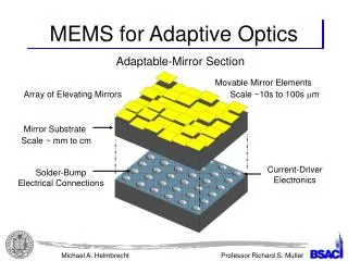
Foundry Process Descriptions MUMPs Metal(0.5 mm) Poly2(1.5 mm) Oxide2(0.75 mm) Poly1 (2.0 mm) Oxide1(2 mm) Poly0(0.5 mm) SiN(0.6 mm) Substrate Trade fill factor, mirror size, array size(wiring depth) Self-planarization may help fill factor $3k 2 mos. SUMMiT MMPOLY3(2 mm) SACOX3(1.5-2 mm, CMP) MMPOLY1+2(2.5 mm) SACOX1(2 mm) MMPOLY0(0.3 mm) SiN(0.8 mm) Oxide(0.6 mm) Substrate Planarization decouples mirror and actuator design etch access holes $10k ? mos.
mirror to actuator vias wiring (MMPOLY0) mirror (MMPOLY3) partial Poly2 self-planarization anchor actuator upper electrode (MMPOLY1+2) etch access holes 3 mm ´ 3 mm flexure 1.5 mm wide Poly1 anchors Incomplete etch of 1.5 mm wide Poly1 gap MUMPs vs. SUMMiT Planarizaton MUMPs self-planarization SUMMiT with CMP Planarization
k, spring constant Movable top electrode d t g V A Fixed bottom electrode Electrostatic Piston Micromirror top electrode, mirror plate to bottom electrode anchor flexure k is a function of flexure number, geometry, and material stiffness (note how unidirectional layout mitigates the effect of residual stress) t is fixed by sacrificial layer thickness of process d is defined by optical modulation requirements Trade k and A for desired V, uniformity, yield, etc. Deflection of electrostatic piston micromirror , for d=0 to ~t/3
Testing Piston Micromirrors Good deflection uniformity on die (wafer) but not necessarily die to die Dynamic laser interferometer testing is expensive in time/complexity 350 With good fit to model, only need one data point for characterization Only need one data point from one device in an array But why not model this simple structure and avoid characterization testing?? Material Properties?? Static fringe measurement V316=18 V 300 250 200 dynamic laser interferometer measured Deflection (nm) modeled 150 100 50 0 0 5 10 15 20 Control voltage (V) Static fringe technique developed for interferometric microscope is very fast Simple procedure: Toggle electrode voltage between 0 and V, fringe lines appear static for deflection=l/2, l,…, where l is test wavelength Interferometric microscope video also provides rapid characterization of yield and deflection uniformity
Segmented MEM-DM (M19) M19 Piston Micromirror Element 12´12 Array 203 mm center-to-center mirror spacing Stroke ~0.6 mm Trapped oxide plate Poly0 wires under flexures Post foundry metallization required Fill Factor: ~77% M19 MEM-DM Image
M1 HeNe Beam Expander MEMS Control PC Aberrating Lens La Optical Attenuator Iris BS2 Ls LM BS1 PSF LF Ll Lw1 Lt2 Lt1 Lw2 Image MEM-DM Optical Power Meter Image Camera PC PSF Camera PC Adaptive Optics Test Bed M19 Optical Measurements Optical input power normalized using attenuator and power meter Increase magnification of far field pattern on PSF camera PSF camera frame rate used to scale measured intensities
Incident Optical Signal Plane ROC=0.80 m ROC=0.35 m Plane 0.07 (174 @40 Hz) 0.04 (108@40 Hz) 1.0 (208@500 Hz) ROC=1.60 m MEM-DM Figure 0.09 (96@99 Hz) 0.76 (158@500 Hz) 0.05 (121@40 Hz) ROC=0.70 m 0.27 (115 @244 Hz) 0.18 (91@203 Hz) 0.04 (97 @40 Hz) M19 MEM-DM Aberration Correction
Status of MUMPs 19 Design • Still have the same device operating in the AFIT AO testbed • Approaching 2 years of intermittent operation exposed to laboratory air • Stan Rogers using to demonstrate phase retrieval • Delivered 2 packaged devices to Dr Wild and Dr Kibblewhite at University of Chicago, Yerkes Observatory • Don’t know status of their work, but recently had inquiry from MEMS Optical who had seen MUMPs 19 devices while visiting U of C • May have a couple left - have been requested by USAF Academy • For quick (~4 months), moderate performance, low-cost devices this design can be shoehorned into a 0.5 cm square die with 4 copies per MUMPs die site • Will yield >50 devices for $3k + packaging costs • Still need post foundry metallization
1011.3 1213.5 120.1 180.4 240.5 202.3 809.0 300.6 360.7 404.5 606.8 Heights (nm) 60.1 1349.0 Height (nm) Height (nm) 378.2 0 203 mm 406 mm 0 203 mm 406 mm 18 V 21 V MUMPs Continuous Facesheet DM Influence Function Observed actuator coupling ~40% in good agreement with predicted Interferometric Microscope Image
MUMPs 21 CF MEM-DM Single element of MUMPs 21 CF DM 144 actuators Wired as a defocus corrector - elements equidistant from center are connected Only 16 voltages required Actuators can flatten residual stress induced deformation etch holes print-through of actuator structure Interferometric microscope images of MUMPs 21 DM center 0 V applied deformation due to residual stress 21 V applied to center 4 elements 21 V applied to 8 elements
Micromirror Surface Figure Potential applications - optical aberration correction - laser communication - direct write photolithography - laser machining - consumer electro-optics Optical Efficiency/ Imaging Performance - fill factor (% reflective surface area) - mirror surface figure -- curvature -- print through -- reflectivity - array surface figure (uniformity) Curvature FF<100% Ideal Print-through Micromirror array surface Far field
MUMPs Mirror Designs All arrays employ 203 mm center-to-center mirror spacing M19 M19_A 12´12 Trapped oxide plate Poly0 wires under flexures Post foundry metal Fill Factor: 77% 8´8 Trapped oxide plate MUMPs metal Fill Factor: 67.4% M19_B M19_C 8´8 Poly2 mirror plate attached to actuator by vias Post foundry metal Fill Factor: 71.9% 8´8 Trapped oxide plate Post foundry metal Fill Factor: 67% MUMPs flexures 4 mm wide for better yield and deflection uniformity
203 mm center-to-center mirror spacing metallization stop & actuator interconnect wiring (MMPOLY0) mirror (MMPOLY3) anchor mirror to actuator vias 10 mm ´ 10 mm actuator upper electrode (MMPOLY1+2) etch access holes 3 mm ´ 3 mm flexure gap 3 mm As-drawn fill-factor: 95% Post foundry metallization required SUMMiT Mirror Design
M19_A False color image of surface height Mesh of surface figure PV=303 nm Scan line Micromirror Surface Characterization Instrument: Zygo Maxim 3-D Laser interferometric microscope Accuracy: 3 nm RMS Manual scan of mirror middle to get Peak-to-Valley (PV) MUMPs devices - only Poly0 electrode under mirror - curvature due to residual material stresses in plate structure - metal ~50 MPa tensile - polys ~10 MPa compressive - trapped oxide ?
SUMMiT False color image of surface height Mesh of surface figure PV=291 nm Scan line Micromirror Surface Characterization SUMMiT - design employs actuator and wiring under mirror plate - planarization incomplete - print-through of underlying structures - some residual stress curvature Zygo results confirmed by checking an unreleased die on stylus surface profilometer Note!: Devices fabricated on early SUMMiT runs Planarization targeted at mechanical vice optical flatness Sandia has now fixed problem (new SUMMiT Optical process)
Optical Perf vs. Micromirror Figure M19_B AFIT Metal 55.6 nm (convex) M19_A MUMPs Metal 303.4 nm PV concave SUMMiT AFIT Metal 291.1 nm PV (print-through + concave) < l/10 Image PSF
Optical Measurement Summary Reflected Optical PSF Mirror Description Optical Efficiency Peak Intensity Effective FWHM Power Normalized Normalized Fill Factor Normalized % % % % % MUMPs Plane Mirror 76.3 100 100 100 100 M19 No Metal 29.2 38.3 5.2 22.8 104 M19_A MUMPs Metal 56.9 74.5 0.6 10.0 221 M19 AFIT Metal 1 62.6 82.0 24.9 49.9 98 M19 AFIT Metal 2 60.8 79.7 25.8 50.8 99 M19_B AFIT Metal 53.6 70.2 35.7 59.8 105 M19_C AFIT Metal 30.0 39.3 7.8 28.0 117 SUMMiT No Metal 44.0 57.7 7.8 28.0 116 SUMMiT AFIT Metal 1 66.0 86.5 7.2 26.7 109 SUMMiT AFIT Metal 2 67.5 88.4 6.9 26.2 111
Surface Figure Study Results Fill factor and optical efficiency (power) not good metrics - don’t measure imaging performance Surface figure is most important factor for imaging performance “Good” polysilicon piston micromirror arrays require - planarization - residual stress control/characterization Sputtered chromium/gold metallization promising Proposed fabrication approach - design in an initial convex curvature using residual stresses - sample lot (release and measure curvature) - design metallization to yield flat mirror surfaces - metallize lot
Latest SUMMiT Optical Design • 32 32 Array of segmented micromirrors (1024 total) • 100 m pitch (center-to-center), Nominal fill-factor ~95% • Employs unproven Row-Column address scheme • Only 2N wires for N2 array • Wiring limits maximum array size in foundry processes • Row-Column (line) addressing demonstrated for bistable mirror arrays • Pulse width & pulse amplitude modulation also demonstrated • (Rounsaval AFIT thesis) • Status • Only a few samples tested - 15 min partial, 30, 45 min release etches (1:1, HF:HCl) • Mirror element flatness <30 nm peak to valley • Unreleased array(s) shows global convex curvature • May be artifact of CMP process, or residual stress in oxide • Probably can minimize by design “tricks” • Can also correct out or “flatten” array in use • Discuss findings with Sandia to determine cause/fix
SUMMiT 32 x 32 Row/Col Array • One array so far had problems with MMPOLY3 attachment to underlying actuators • May suggest non-uniformity of CMP oxide thickness across wafers • Have heard CMP “wedge” problem anecdotes Actuator-only global curvature is convex (~120nm peak to valley)
Interferometer Images MUMPs 19 = 632 nm MUMPs Plane Mirror (Gold) SUMMiT Optical
Testbed Images & PSFs (Preliminary data) SUMMiT Optical Partial Release(?) MUMPs Plane Mirror (Gold) SUMMiT Optical Full Release (30/45?) MUMPs 19
Proposed CfAO SUMMiT Design • 128 to 256 element array of segmented micromirrors • Single wire per element address scheme (die size/wire bond limited design) • Wire-bonded electrical connections • Minimum 100 m pitch (center-to-center) • Larger element size for increased fill & lower operating voltage • Have 128 element 203 m designs on 0.5 cm square die • Trade of bond pad space & mirror size required to optimize • Minimum fill-factor ~95% • Minimum stroke: 0.5 m • Mirror element flatness <30 nm peak to valley • Optimize global flatness by design and study of process using current arrays • Status • Have had initial discussions with Sandia about approach • Want design that they will agree to release/package/bond • Standard module run should yield 50-75 finished parts (untested) • Will explore progress of metallization - use if available • Otherwise design for ease of post-foundry (user) metallization