Download
1 / 1
20 likes | 279 Views
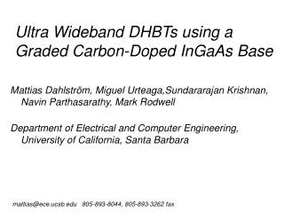
70 Å GaAs:Si, N D = 2 10 18 cm -3. 350 Å Al 0.3 Ga 0.7 As. D1 Å GaAs:Si, N D = 2 10 18 cm -3. D2 Å In x Ga 1-x As, - doped Si. D1 Å GaAs:Si, N D = 2 10 18 cm -3. 350 Å Al 0.3 Ga 0.7 As. 100 Å GaAs:Be, N A = 1.5 10 18 cm -3. 2000 Å GaAs buffer.

E N D
70 Å GaAs:Si, ND = 21018 cm-3 350 Å Al0.3Ga0.7As D1 Å GaAs:Si, ND = 2 1018 cm-3 D2 Å InxGa1-xAs, - doped Si D1 Å GaAs:Si, ND = 2 1018 cm-3 350 Å Al0.3Ga0.7As 100 Å GaAs:Be, NA = 1.5 1018 cm-3 2000 Å GaAs buffer GaAs S-I substrate (100) Low Thermal Drift in Highly Sensitive Doped-ChannelAlGaAs/GaAs/InGaAs Micro-Hall Magnetometer Vas. P.Kunetsa), J. Dobberta,c), Yu. I. Mazura), H. Kostialb), E. Wiebickeb), U. Müllerc), W. T. Masselinkc), G. J. Salamoa) a) Physics Department, University of Arkansas, Fayetteville, AR, USA; b) Paul-Drude-Institute, Berlin, Germany; c) Humboldt University, Berlin, Germany Motivation Theory and Experiment Additional Advantages Biology and Medicine Magnetic Labeling of Molecules Material and Physics Science The structures were optimized for thermal stability by solving the Shrödinger-Poisson equation self-consistently 1). Typical sub-micron devices will suffer from carrier depletion and non-uniform distribution of the electric field 2). Magnetic Recording Media T. Schweinböck, PhD Thesis, Regensburg (2001) Scanning Hall Probe Microscopy (SHPM) Magnetotactic Bacteria R. Dunin-Borkowski et al.: Science 282, 1868 (1998) Nano-Functional Materials Humboldt University, Berlin (2004) InMnAs Dot Chains, E. Marega Jr. and Greg Salamo (2007) Neuroscience H. Yabuki :Japan, IPCR 1. Non-Destructive Method 2. Sensitive Method (nano-T or pico-T sensitivity) 3. Quantitative Method 4. Room Temperature Operation Optimization of geometry and the use of the doped channel devices will result in improved operation at high electric fields 3). The Hall effect measurements of the electron mobility and density exhibit thermal stability of 192 ppm/0K (voltage drive mode) and 90 ppm/0K (current drive mode), respectively. Device Fabrication The device structures were grown by MBE. The total thickness of the 2D1+D2 channel was keptto350 Å. The growth temperatures for GaAs, AlGaAs and InGaAs were 580 0C, 610 0C and 560 0C, respectively. micro-Hall device The sensitivity and noise measurements reveal detection limits of 438 nT at 10 kHz and 300 K for 144 Å InGaAs QW 2) Vas. P. Kunets et al., J. Appl. Phys. 98, 094503 (2005) 3) Vas. P. Kunets et al. Sensors and Actuators A 101, 62 (2002) Conclusions The doped channel micro-Hall devices based on high electron velocity materials exhibit excellent thermal stability, low noise, high sensitivity, and the ability to operate at high electric fields. The direct doping of the channel may be an alternative for sub-micron devices and also a solution for narrow band gap materials like InSb and InAs, which suffer from thermal drift. Dry chemical etching for mesa definition and Au/Ge/Ni for metallization. Transmission Line Model 1) 1D Poisson-Shrödinger Band Diagram Calculator, by Greg Snider (Notre Dame) This work was supported by National Science Foundation through grant DMR-0080054 and DFG Grant MA 1749/4-1(2)