Download
1 / 50
500 likes | 698 Views
5-5- High power switching systems Which includes: 5-5-1 general thyristor Characteristics. 5-5-2 DC switching circuits. 5-53 AC switching circuits. Learning Objectives. At the end of this topic you will be able to;. 5-5-1. 5-5-2. 5-5-3. General Thyristor characteristics.

E N D
5-5- High power switching systems Which includes: 5-5-1 general thyristor Characteristics. 5-5-2 DC switching circuits. 5-53 AC switching circuits.
Learning Objectives.At the end of this topic you will be able to; 5-5-1 5-5-2
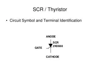
General Thyristor characteristics. The thyristor is a three-terminal device, made from a semi-conducting material. The diagram shows the circuit symbol and identifies the three terminals.
It is also known as a silicon controlled rectifier, which describes its DC behaviour very well. It is a special type of diode that allows current to flow only when a control signal is applied to its gate. Once turned on, the thyristor will not turn off, even after the gate signal has been removed, provided a sufficiently large current flows through the it from anode to cathode..
A typical arrangement for switching on a thyristor in a DC circuit is shown in the next diagram. When the switch S is closed, a current IG flows into the thyristor gate. Providing this current is big enough, i.e. bigger than a value known as the minimum gate current, IGT, typically between 0.1 mA and 20mA, the thyristor will switch on. Similarly, the voltage applied between the gate and the cathode, VG, must be greater than a value, called the minimum gate voltage, VGT. This is typically between 0.6V and 1.0V.
The thyristor then latches on, and so a current, IA, flows through the load even when switch S is opened again. However, if this current drops below a minimum value, called the holding current, IH, the thyristor switches off and no more load current flows. Typically, IH is around 10mA. A resistor, R, is used to protect the thyristor gate from excessive current. To calculate a suitable value for R, use the minimum values of gate current and voltage to calculate a maximum value for R.
DC Switching Circuit: Before looking at the switching properties of a thyristor, we look back at the behaviour of a switching circuit, in particular, the power dissipated in the switch.
In other words, in both the ‘off’ and ‘on’ states, there is no power dissipated in the switch. It does not overheat. It is not damaged. We have assumed that this is a perfect switch, with infinite resistance when open, and zero resistance when closed, and that it changes instantly from one state to the other! The power dissipated in the switch is zero throughout, only if the current is zero when there is a voltage across the switch, and the voltage across the switch is zero when a current flows through it. We must avoid any situation where there is both a non-zero current and non-zero voltage across the switch.
Let’s look at the transistor as a switching device in this context. The transistor behaviour is controlled by the voltage, VIN, applied to the base. ( More accurately, it is controlled by the current flowing in the base.)
Typically, when VIN rises to about 0.5V, the transistor starts to switch on, and conduct appreciable current. By the time VIN has reached around 1.0V, the transistor is switched on fully. This behaviour is shown in the graph.
The problem is the region of the graph between VIN = 0.5V and VIN = 1.0V. In this region, the transistor is neither off nor on. It is starting to conduct, so the current I is growing. It is not switched on fully, so voltage V1 is not zero. As a result, the transistor is dissipating power. It is getting hot! (The only major weakness for semiconducting materials is that they cannot tolerate high temperatures.) The ideal switching device is one which moves very rapidly from ‘off’ to ‘on.’ The transistor is not good at this. With very high currents and voltages (high power,) transistors do not make good switching devices.
Thyristors, on the other hand, make superb high power switching devices. They move extremely quickly from the forward-blocking state, where the device is forward-biased, but not conducting, into the conducting state when it receives a sufficient gate pulse. As a result, it dissipates very little power in the process.
In the conducting state, there is a residual voltage drop of around one volt between anode and cathode, VAK, so there is still some power dissipation, which may mean that the device has to be cooled in some way (by use of a heat sink for example.) As a switching device, the thyristor has another major advantage over a transistor. It is a self-latching switch. Once the device is switched on, (and passing a current larger than the holding current,) the gate signal can be removed. With a transistor switch, a collector current flows only while the base current is present. Remove the signal from the base and the transistor switches off.
In some ways then, the thyristor behaves like a self-latching relay. However, the thyristor is a solid-state device. It has no moving parts to wear out through friction, unlike the relay. Its switching takes place in microseconds, compared to the tenths of a second that it takes the relay contacts to close. Like the relay, it is capable of handling high currents.
Capacitor commutation: Once triggered into the conducting state, the basic thyristor cannot be turned off by signals applied to the gate. (In other devices, such as the GTO (gate-turn-off thyristor, this is not true.) The standard thyristor turns off only when either: • the anode-cathode current falls below the holding current threshold;or • the device is reverse-biased – with the anode being less positive than the cathode.
The customary way to switch off a thyristor in a DC switching circuit is to use capacitor commutation. The circuit diagram for this is shown below. We are using a supply voltage of 12V, only to help with the description of what happens. Any reasonable supply voltage can be used.
Suppose that we start from the beginning, with the thyristor switched off. The full supply voltage, VS, sits across the thyristor. In other words, the voltage at point P = +12V. The voltage drop across the load is zero, and no current flows through it. Switch S2 is open, and so the voltage at Q = VS = +12V. Next, switch S1 is pressed, sending a pulse of current into the gate. This switches on the thyristor. The voltage at P drops to 0V (nearly) and the supply voltage now appears across the load, causing a current to flow through it. Switch S1 can be released because the thyristor is latched on. The voltage at Q = +12V still.
The capacitor has a voltage of 0V on its left-hand terminal, and +12V on its right-hand terminal. Put another way, Q sits 12V higher than P. The significant feature about capacitors is that the voltage drop across them cannot change until charge flows to or from one of the terminals. If we suddenly change the voltage of one terminal, the other one must change by the same amount until there is time for charge to flow to adjust that voltage.
To switch off the thyristor, switch S2 is pressed for an instant. As a result, the voltage at Q falls to 0V. However, there has been no time for charge to move. As a result, Q must still be 12V higher than P. In other words, when the voltage at Q dropped by 12V from 12V to 0V, the capacitor forced the voltage at P down the same amount, from 0V to -12V. Looking at the thyristor, the anode, connected to P, is now at around -12V, while the cathode is connected to 0V. We have reverse-biased it. It switches off.
In reality, the voltage at P may not reach -12V. That does not matter. All that is needed is that it drops below 0V to reverse-bias the thyristor. The load usually has a low resistance, and so when the thyristor switches off, a large current flows through the load and onto the left-hand plate of the capacitor. The voltage at P rises quickly to +12V. Similarly, when S2 is released, current flows through the pull-up resistor R2, returning the voltage at Q to +12V.
AC Switching Circuit: The issues in an AC circuit are different. It is not difficult to switch off the thyristor – it becomes reverse-biased during every cycle of the supply, when the current direction reverses! The problem is to keep turning it on. One way to do this, called phase control, is shown in the circuit diagram. Consider the two parallel limbs of the circuit separately.
PHASE SHIFTING We could use a resistor-capacitor chain across the supply to control the magnitude and phase of the gate voltage. Consider an AC signal of the form V = Vo sin 2πft being applied across an RC circuit
1. Capacitor and variable resistor: The capacitor is connected to the AC supply through the variable resistor. It tries to charge up and then discharge so that the voltage across it, VC, follows the supply voltage. When the variable resistor is set to zero, VC follows the AC supply exactly (shown in the middle graph.) When the variable resistor offers some resistance to the flow of current, the capacitor is not able to charge and discharge fast enough, and so a phase lag is created between VC, and the supply voltage, VS, ( shown in the bottom graph.) This phase shift can be specified as an angle f with value between 00 and 900
2. Thyristor and load: Now look at the limb of the circuit containing the thyristor and the load. The gate terminal is connected to the top of the capacitor, and so follows voltage VC. Providing that the thyristor is forward-biased, it will switch on as soon as the voltage across the capacitor, VC, reaches the minimum gate voltage, VGT. It switches off when it becomes reverse-biased.
When switched on, the voltage across the thyristor, VT, is (ideally) 0V, and so all the supply voltage appears across the load. When switched off, all the supply voltage appears across the thyristor, and so the voltage across the load, VL, is zero, and no current flows. Study the graphs opposite and compare them with the descriptions given above.
Exercise 3 (The solutions are given at the end of the topic.) Calculate the phase angle produced in the phase control circuit shown opposite when the variable resistor is set to a resistance of 50kW.
Improved AC Switching Circuit: An improved switching arrangement relies on the properties of a device called a diac. This behaves rather like a double zener diode. It does not conduct until the voltage across it exceeds a certain level, known as the breakover voltage. Above this, it conducts freely, offering very little electrical resistance. This behaviour is shown in the current/voltage graph.
The important thing is that switching occursas rapidly as possible, to reduce powerdissipation in the thyristor. The voltage, VC,across the capacitor rises relatively slowly, ascan be seen in the graphs shown on earlier pages. Adding a diac, as shown in the circuit diagram, makes the switch-on sharper. Other advantages of this arrangement are that it overcomes the variability in switch-on. This is due to two factors. Firstly, these devices are mass-produced, and so there is variability in their operating parameters. Secondly, the switch-on voltage varies slightly with temperature. The breakdown voltage of the diac, around 30V, is high enough to mask any effects due to mass-production and temperature variation.
The graphs show the effect on the thyristor and the load of using a 30V diac in the triggering circuit.