Download
1 / 19
190 likes | 350 Views
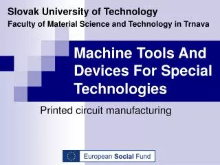
Slovak University of Technology Faculty of Material Science and Technology in Trnava. Machine T ools A nd D evices F or S pecial T echnologies. Printed circuit manufacturing. Printed circuit manufacturing.

E N D
Slovak University of Technology Faculty of Material Science and Technology in Trnava Machine Tools And Devices For Special Technologies Printed circuit manufacturing
Printed circuit manufacturing Printed circuits are circuits between components created of conductivity layer strong connected wih support layer of isolant. Printed circuit board (PCB) be able to: • Single sided – on one’s side of raw material is created conductible network by copper layer, • Two sided – conductible network is establishing on both sides of raw material, • multilayer – they have more than two conductive layers and on each is establishing conductive pattern, • By photosensitive coat – on copper film is deposited photosensitive layer, • Universal bored – they have created metal-coated holes.
Printed circuit manufacturing - • With constructional class the costs are increasing • By technology of silk print process are made single-layer and two-layer PCB until III. design class. • Multilayer boards are made only by design class IV, V and VI.
Printed circuit manufacturing by silk print process and photo way Etch resistant pattern on copper foil is created: • that special silk printing colour is extrude by silk printing template to board • By special photosensitive emulsions Photo way is more-accurately as silk print process.
Using of silk printing a – automatic line, b – hand silk printing
Particular production technology • Manufacturing one or two-sided PCB by silk printing without metallized holes • Manufacturing one or two-sided PCB by photo way, without metallized holes • Flexible printed circuit manufacturing
PCB surfacing Printed circuit board coating increase corrosion resistance of cooper foil free part and restrict contact resistance increasing at corrosion. Galvanizing increase the connector parts abrasion resistance.
Types of PCB surfacing • Galvanic metallization, • Tinning, • HAL, • Deposition of photosensitive mask, • Deposition of detachable protecting cover, • Soldering flux deposition, • Stripping.
Galvanic metallization Surface metallization is able to execute by two ways, namely negative and positive. By positive way are printed circuit metallized till after etching. At negative electro galvanizing is on non-etched material at first made contact pattern from galvanically resistant mask and only contacts stay naked and they can electro galvanize its.
Tinning • PCB surface treatment, where is depositing tin (SN60PB) in hot on tinning devices • Deposited layer thickness is between 0,015 till 0,02 mm • Tinning boards width is limited and not allowed get over than 280 mm. Length is unlimited.
HAL (Hot Air Leveling) • standard procedure in the PCB production process, • levelling by hot air, • depositing the coat of solder from Sn-Pb eutectic composition from melting
Deposition of photosensitivemask and of detachable protecting cover Mask is coated to printed circuit board by silk printing.
Soldering flux deposition Fluxing agent – fluid applied before soldering on metal surface to surface protection before oxidation and to provide good solderability.
Stripping • Removing the coating from material surface. • Stripper is utilise to tinning layer removal, whereby stay PCB only with copper surface and is possible apply soldering mask.
PBC controlling • is realising as a final step of manufacturing technology. PBC control station