Download
1 / 15
150 likes | 172 Views
Explore detailed considerations and optimizations for power delivery in readout plane design for efficient functioning. Covering topics like power consumption, local decoupling networks, transient responses, and more.

E N D
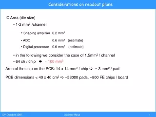
Considerations on readout plane • IC Area (die size) • 1-2 mm2 /channel • Shaping amplifier0.2 mm2 • ADC 0.6 mm2 (estimate) • Digital processor 0.6 mm2 (estimate) • in the following we consider the case of 1.5mm2 / channel • 64 ch / chip ~ 100 mm2 • Area of the chip on the PCB: 14 x 14 mm2 / chip ~ 3 mm2 / pad • PCB dimensions < 40 x 40 cm2 ~53000 pads, ~800 FE chips / board
Digital PWR planes Analogue PWR planes Chip floorplan amplifiers ADCs Digital Processing Considerations on readout plane PCB topology and layer stack-up 8-layer PCB vdd Digital signals II gnd Digital signals I gnd det gnd Pad signals routing Pad layer Flip-chip mounted PCB
Considerations on readout plane • Power consumption • amplifier 8 mW / channel • ADC 30 mW / channel • Digital Proc 4 mW / channel • Power regulation and links 10 mW / channel • duty cycle: 1% • average power / channel ~ 0.5 mW / channel • average power / m2 167 W
Considerations on readout plane Readout Board power delivery network ON/OFF RO CHIP Large storage capacitors Model used to evaluate the impedance of the local power delivery network VRM can be turned off High optimization of local decoupling network is required Impedance (W) versus frequency for the local power delivery network connected to the RO chip through a power plane with zero inductance.
R = 2 x 3.4 mW, DV = 1.32V R = 2 x 6.8 mW, DV = 816mV Voltage on load (V) I stdby (A) I max (A) Bus bar Section (mm2) Bus Bar description What is the transient response of the bus bar? Analogue4.0 60 60 100 Digital3.3 133 194 200 TPC Low Voltage Distribution Scheme TPC endplate Wiener power supplies L ~ 11mH 121 FEE Cards DIGITAL Bus Bar pair (positive + return line) 115A max DIGITAL 115A max 40m Bus Bar pair ANALOGUE 115A max
60A (15A / ms) Dynamic Digital Current Consumption 3.3V 2.5V Power Supply Regulator ALTRO 100 µF 1 µF 10 × 100 nF Standby power 4 ms peaking time
60A (0.6A / ms) Dynamic Digital Current Consumption 3.3V 2.5V Power Supply Regulator ALTRO 100 µF 1 µF 10 × 100 nF Standby power 100 ms peaking time
ILoad DI THigh time Test setup 40m I Electronic Load HP6050A – 6050B Wiener PL500 VPS VLoad multi-strand copper bar h=1cm R C • = 2.110-8Wm L = 11mH F = 160mm2 Test Configurations Configuration A: R = C=0 Configuration B: R=25mW C=0; Configuration C: R=25mW C=70mF Configuration D: R = C=70mF
62.6V 680mV 0.8ms Measurement 1 (configuration A ) Test Parameters DI (A)Freq (Hz) DTHIGH (ms)Slew rate (A/ms) 60 100 4 10 A sudden interruption of the current can damage the Front End Cards !
Measurement 2 (configuration B ) Test Parameters DI (A)Freq (Hz) DTHIGH (ms)Slew rate (A/ms) 41.6 100 4 10 A current swing of 41.6A produces a transient voltage of ~1.8V t = L/R ~ 1ms 0.78V 480mV • Voltage drop across the bar for a current swing of 60A • DV low load (dc) 0.90 V • DV high load (dc) 1.32 V • DV (transient) 3.40 V 1.28V
Measurements 3 (configuration C ) Test Parameters DI (A)Freq (Hz) DTHIGH (ms)Slew rate (A/ms) 41.6 100 4 10 “ 1000 0.1 “ A A B B B A ALICE TPC conditions 0.95V 0.30V 70mF in parallel to the electronic load assorbes the large transient spikes
Test Parameters DI (A)Freq (Hz) DTHIGH (ms)Slew rate (A/ms) 60 10 40 10 Measurements 4 (configuration D ) 2V
Measurements 5 (configuration A + sense wire ) The sensing feedback is not fast enough to react to the load variations Test Parameters DI (A)Freq (Hz) DTHIGH (ms)Slew rate (A/ms) 60 100 4 10 “ 1000 0.1 “ A A B B B A ALICE TPC conditions 3.3V 2.5V 100ms
Measurements 6 (configuration C + sense wire ) The sensing feedback is not fast enough to react to the load variations Test Parameters DI (A)Freq (Hz) DTHIGH (ms)Slew rate (A/ms) 41.6 100 4 10 1.2V
Measurements 7 (configuration C + sense wire ) The sensing feedback is not fast enough to react to the load variations Test Parameters DI (A)Freq (Hz) DTHIGH (ms)Slew rate (A/ms) 41.6 1000 0.1 10 C = 100mF 100ms 220mV