Download
1 / 11
110 likes | 243 Views
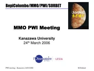
MMO PWI Meeting Kanazawa University 24 th March 2006. SORBET instrument overview. Analogue front end status. Design of a simplified BBM including the main functionalities of the receiver 2 channels receiver using discrete and ASIC technology on the same PCB board

E N D
MMO PWI Meeting Kanazawa University 24th March 2006 M.Dekkali
SORBET instrument overview M.Dekkali
Analogue front end status Design of a simplified BBM including the main functionalities of the receiver • 2 channels receiver using discrete and ASIC technology on the same PCB board • Technical evaluation of the both options (discrete and integrated) • Functional testing has been done and show the ASIC feasibility • Performances are better using the ASIC • The ASIC will greatly help to minimize the power budget (at least –300mW) Still to be done • Thermal and radiation evaluation (2Q/2006) • Confirmation (or not) of the ASIC option (3Q/2006) • ASIC in its final configuration – 3rd version (4Q/2006) • BBM including all the functionalities of SORBET (4Q/2006) • Qualification of the last ASIC version (2007) M.Dekkali
New ASIC design (January 2006) Analogue functions on a single chip : • Specific for SORBET (Full Custom design) • Thin CMOS technology (AMS 0.35um) • Logarithmic amplifiers (AGC) • Low noise mixers • Selective band-pass filter • Low noise operational amplifier Functional testing showed : • Measurements and simulations match very well • Improvement of the AGC dynamic range • AGC response less linear but still acceptable • Reduction of the power consumption Future actions • Thermal testing (soon) • Radiation evaluation (2Q/2006) • Decision to continue the ASIC solution (3Q/2006) 2.6mm 2.6mm M.Dekkali
Analogue front end test bench Plot of the receiver response as a function of the input level or the frequency Test bench for analogue purposes : • 2 channels acquisition module • User I/F – BuilderC++ environment • Receiver setup • Stimuli control • GPIB and USB Interfaces • Data acquisition and storage • Graphic display • Manual and automatic tests (scripts) M.Dekkali
Radiation testing plan Preliminary radiation tests for an early evaluation of the ASIC technology Objectives : • Early detection of possible failures • Evaluation of the technology limits regarding the SEL and the TID • Make a decision about the ASIC option Latch-up tests : • Tests on 1 ASIC sample powered ON • Heavy ions beam at Louvain (Belgium) • Monitoring of the power supply for latch-up detection Total dose tests : • 7 ASIC under radiation (5 ON + 2 OFF) + 1 sample for control • CO-60 source up to 100kRad (testing facilities still TBD) • Anneling (ASIC ON @100°C during 160H) and final tests Applicable documents : • ESA/SCC specification N°25100 (for SEL) and N°22900 (for TID) • Radiation testing plan (TBW) M.Dekkali
Digital Unit : hardware First BBM design (still under development) : • A6 size daughter board • Re-programmable 2 millions gates FPGA (XILINX) • 128KB low power Honeywell SRAM (+128KB option) • 64KB EEPROM • SpaceWire interfaces (2.5V and 3.3V transceivers) • 2 channels S&H + ADC (AD9225 or HMXADC9225) • Local 1.5V / 2.5V voltage regulator • External 3.3V / 5V / ±12V • Testing connectors : 48 logic analyzer channels, RS232 DSU for LEON M.Dekkali
Digital Unit : FPGA design Low power processor : • Leon 2 LGPL : control, commands, DSP, data compression Configuration: 1KB dcache, 1KB icache, MAC16x16, DSU, 32 interrupts controler => Solution for SEU-free: LEON2FT? LEON3FT? • Spw-b-2.0 (ESTEC) mapped in IO area: MDP communication Configuration: SysClock=3MHz, SlowClock=10MHz, SDR, 32 FCT • Pseudo random noise : internal calibration • ADC module : sampling sequences, data buffering • Analog setup module : receiver configuration • Synthesizer controller : to be written M.Dekkali
Digital Unit : development tools • FPGA tool chain : Windows (Actel) and Linux Redhat (Xilinx) • External/Internal logic analyzers : HP16900/ChipscopePro • Software development tools : Eclipse + CDT + GRMON evaluation / sparc-elf-gcc / ddd • SpaceWire tools : USB-brick (2 ports through USB) Java tests application (Dundee) M.Dekkali
Interfaces with PWI I/F update : • 3cm slot in the MDP chassis • Confirmation of the analogue +5V • DC-DC converters switching frequency • Shield between the PSU and others PWI instruments • Grounding to the MDP chassis • Connection between sensors and instruments Other : • Energy distribution of the particles at Mercury M.Dekkali
Power supply budget (TBC) Bus Power ------------------------------------------ +12V 0mW -12V 100mW +5V 700mW -5V 0mW (TBC) +3.3V 450mW ------------------------------------------ Total 1250 mW M.Dekkali