Download

1 / 1
0 likes | 6 Views
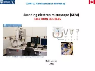
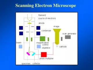
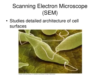
The Global Critical Dimension Scanning Electron Microscope (CD-SEM) Market is set for substantial growth from 2023 to 2030, driven by the increasing demand for precise measurement and inspection in semiconductor manufacturing and nanotechnology. CD-SEMs are essential for advancing the fabrication of integrated circuits and electronic components. Factors such as technological advancements, the miniaturization of electronic devices, and the growing focus on quality control in production processes are propelling market expansion.<br><br>

E N D
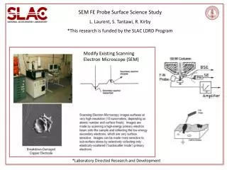
+1 217 636 3356 +44 20 3289 9440 sales@mobilityforesights.com Company Market Reports Consumer Research Advisory Services Exports - Imports Careers Contact Us Blog Your Name Business Email Global Critical Dimension Scanning Electron Microscope Market 2023-2030 Country Phone Number +49 Company Name Single User License : $ 4,000 Your message Corporate User License : $ 6,000 By submitting this form, you are agreeing to the Terms of Use and Privacy Policy. Request Sample I'm not a robot reCAPTCHA Privacy - Terms BUY NOW DOWNLOAD SAMPLE DESCRIPTION TABLE OF CONTENTS GLOBAL CRITICAL DIMENSION SCANNING ELECTRON MICROSCOPE MARKET INTRODUCTION A Critical Dimension SEM (CD-SEM: Critical Dimension Scanning Electron Microscope) is a dedicated system for measuring the dimensions of the fine patterns formed on a semiconductor wafer. CD-SEM is mainly used in the manufacturing lines of electronic devices of semiconductors. Scanning electron microscope measurement of width and shape of 10nm patterned lines using a JMONSEL-modelled library. Ultramicroscopy. Sometimes it’s a diamond, or an oval, or simply an asterisk next to the dimension. Three main CD-SEM features that differ from the general-purpose SEM:CD-SEM primary electron beam irradiating to the sample has low energy of 1keV or below. Lowering the energy of the electron beam of CD-SEM can reduce the damage to the sample due to charge-up or electron beam irradiation. CD-SEM measurement accuracy and repeatability is guaranteed by improving magnification calibration to the maximum extend. Measurement repeatability of CD-SEM is around 1% 3σ of the measurement width. Fine pattern measurements on the wafer are automated. A sample wafer is put inside a wafer cassette (or a Pod / FOUP), which is placed on the CD-SEM. The condition and procedures of the dimensional measurement are input into a recipe* in advance. When the measurement process is started, the CD-SEM will automatically take the sample wafer out of the cassette, load it into the CD-SEM and measure the desired positions on the sample. When the measurement is finished, the wafer will be returned to the cassette. GLOBAL CRITICAL DIMENSION SCANNING ELECTRON MICROSCOPE MARKET SIZE AND FORECAST Global critical dimension scanning electron microscope market accounted for $XX Billion in 2022 and is anticipated to reach $XX Billion by 2030, registering a CAGR of XX% from 2023 to 2030. RECENT DEVELOPMENTS Recent developments in scanning electron microscope design. some improvements in scanning electron microscope (SEMs) resolution with respect to the redesign of its electron lenses. By suitably redesigning a SEM’s electron lenses, the on-axis aberrations of the objective lens have typically been reduced by over one order of magnitude, and the resolution has been improved by more than a factor of three. Significant progress has been made, particularly with respect to low voltage scanning electron microscopy. Another area of development is the miniaturisation of the scanning electron microscope. Miniature high-resolution electrostatic columns have been proposed for low-voltage applications that measure only a few millimetres high, while permanent magnet miniature columns have been designed that have heights less than 100 mm. COMPANY PROFILE HITACHI SPIE ACS Frontiers SERc THIS REPORT WILL ANSWER FOLLOWING QUESTIONS 1. How many critical dimension scanning electron microscopes are manufactured per annum globally? Who are the sub- component suppliers in different regions? 2. Cost breakup of a Global critical dimension scanning electron microscope and key vendor selection criteria 3. Where is the critical dimension scanning electron microscope manufactured? What is the average margin per unit? 4. Market share of Global critical dimension scanning electron microscope market manufacturers and their upcoming products 5. Cost advantage for OEMs who manufacture Global critical dimension scanning electron microscope in-house 6. key predictions for next 5 years in Global critical dimension scanning electron microscope market 7. Average B-2-B critical dimension scanning electron microscope market price in all segments 8. Latest trends in critical dimension scanning electron microscope market, by every market segment 9. The market size (both volume and value) of the critical dimension scanning electron microscope market in 2023-2030 and every year in between? 10. Production breakup of critical dimension scanning electron microscope market, by suppliers and their OEM relationship RELATED REPORTS Global LED Strip Lights Market 2022-2027 Global GaN Converter Market 2022-2027 Global Proximity Sensors Market Size and Forecasts to 2030 $4,000 $4,000 Multi User Multi User $3,500 Multi User License - License - MARKET REPORTS CONSUMER RESEARCH INFORMATION ADVISORY SERVICES CONTACT INFORMATION 172/1, 2nd Floor, 5th Main, 9th Cross Automotive and Transportation About Us Focus Group Study Transaction Advisory Rd, Opposite to Kairalee Nikethan Semiconductor Our Clientele Education Trust, Indira Nagar 1st Stage, Ethnographic Market Positioning Agriculture and Construction Our People Bengaluru, Karnataka 560038, INDIA Research Assessment Equipment Blog Brand Awareness Custom Automotive Aerospace and Defense +1 217 636 3356, +44 20 3289 9440 Contact us Study Market Research Marine and Rail Terms & Conditions sales@mobilityforesights.com Consumer Satisfaction Strategic Advisory Logistics and Packaging Privacy Policy Survey Competitive Working Hours: Mon - Fri (9 AM - 9 PM Medical Devices ESOMAR Guidelines Consumer Expectation Intelligence IST) Chemical and Materials Compliant & Loyalty Assessment Electrical Machinery Connect with us ICT Energy, Power and Robotics New Technologies © Copyright 2017-2023. Mobility Foresights. All Rights Reserved. 0