Download
1 / 35
380 likes | 621 Views
Learn about the features, operating modes, CPU features, and key registers of the MC68HC11 microcontroller introduced by Motorola for low-power consumption and high performance operation. Discover its applications and salient features in this comprehensive guide.

E N D
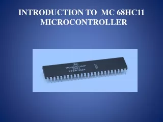
INTRODUCTION • Motorola Inc ,one of the pioneers in microcontroller manufacturing has introduced this 8-bit microcontroller M68HC11 in the year 1985 and it is descended from the Motorola 6800 microprocessor. Now it is produced by Freescale Semiconductors. • It is a CISC microcontroller , optimized for low power consumption and high-performance operation.
Contd.. • The 68HC11 chip has built-in EEPROM/ROM, RAM, digital I/O, timers, A/D converter, PWM (Pulse width modulator) generator, and synchronous and asynchronous communications channels.
OPERATING MODES The 6811 can operate in one of the four modes: • Single-chip mode: uses internal memory for program & data. • Expanded mode :allows for use of external memory. • Bootstrap mode: used to load programs into RAM. • Test mode : used by Motorola to test the chip is operation
SALIENT FEATURES • The HCMOS MC68HC11 is an advanced 8-bit MCU with numerous on-chip peripheral capabilities. • Up to 10MIPS Throughput at 10MHz • 256 Bytes of RAM , 512 Bytes of In-System Programmable EEPROM. • Eight channel 8-bit Analog to Digital Convertor • One serial peripheral interface, with a speed up to 1M (baud rate)
Contd… • The MC68HC11 is available in two packages . • One is 48-pin dual inline package (DIP) and the other is the 52 Pin Plastic Leaded Chip Carrier(PLCC) known as Lead quad pack. • In the 48 pin DIP package 38 pins are available for I/O functions.(34 I/O lines+ 2 interrupt lines + 2 hand shake control lines). • Similarly in a 52 PLCC pack 42 pins are meant for different I/O functions, and the remaining are used for interrupt and handshake signals.
Contd.. • MC68HC11 has one universal Asynchronous Serial Communications Interface (UART) • Six powerful addressing modes (Immediate, Extended, Indexed, Inherent and Relative) • Power saving STOP and WAIT modes • Memory mapped I/O and special functions
It is based on HCMOS Technology and has a common internal bus for the address and data of 8-bits. • It has an MCU clock whose frequency can be reduced to zero. As the MCU is completely MOSFET based the power dissipation is negligible in stop or start states. So, this is optimized for lowpower consumption and high performance operation.
CPU FEATURES • An 8MHz XTAL(external clock) with 2 MHz clock related operations. • A 16-bit program counter that loads a powerup value from a reset vector address 0xFFFE – 0xFFFF • Two 8- bit Accumulators A and B work as general purpose registers. They can be concatenated as a 16-bit double accumulator [D]. • Two 16-bit Index registers Ix and Iy can be used as pointers to memory locations and hold the 16 bit addresses of memory locations .
Contd.. • It has a multiplexed address and data bus. • One 16 –bit stack pointer ,which decreases by 1 after the push of each byte. • Two external interrupts IRQ ,XIRQ .One of this can be configured as non-maskable external interrupts. • Although this is an 8-bit processor ,it has some 16-bit instructions.(ADD,Sub,shift and rotate)
68HC11 Registers • The MC68HC11 microcontroller has a rich set of registers and they are classified into two categories : CPU registers and I/O registers. • The CPU Registers are shown in the next slide. A and B are the two 8-bit registers called general purpose accumulators which are used to perform most of the arithmetic operations. These two accumulators can be concatenated to form a 16-bit accumulator which is known as double accumulator “D”. This accumulator is used for 16 bit operations.
Contd.. • Index registers (IX and IY).Two 16-bit registers used mainly in addressing memory operands. They normally used to hold addresses of 16-bit memory locations.These registers are also , some times used for them for 16-bit computation also. • Stack Pointer (SP):Stack is a first in first out data structure.This 16-bit stack pointer register hold the address of the stack top.
Program Counter(PC): It is a 16-bit register which stores the address of the next instruction to be executed. The 68HC11fetches the instruction one byte at a time and increments the PC by 1 after after fetching each instruction byte. After the execution of an instruction the PC is incremented by the number of bytes of the executed instruction.
Condition Code Register (CCR) • This is an 8-bit register used to keep track of the program execution status , control the execution of conditional branch instructions and enable/disable the interrupt handling . • This register contains five status indicators, two interrupt masking bits, and a STOP disable bit. The register is named for the five status bits since that is the major use of the register.
Contd.. • These status flags reflect the results of arithmetic and other operations of the CPU as it performs instructions. The five flags are half carry (H),negative (N), zero (Z), overflow (V), and carry/borrow (C). The half-carry flag, which is used only for BCD arithmetic operations is only affected by the add accumulators A and B (ABA), ADD, and add with carry (ADC) addition instructions
Contd.. • The N, Z, V, and C status bits allow for branching based on the results of a previous operation. Simple branches are included for either state of any of these four bits. The H bit indicates a carry from bit 3 during an addition operation. This status indicator allows the CPU to adjust the result of an 8-bit BCD addition so it is in correct BCD format, even though the add was a binary operation. This H bit, which is only updated by the ABA, ADD, and ADC instructions, is used by the DAA instruction to compensate the result in accumulator A to correct BCD format.
Contd.. • The N bit reflects the state of the most significant bit (MSB) of a result. For twos complement, a number is negative when the MSB is set and positive when the MSB is 0. The N bit has uses other than in twos-complement operations. By assigning an often tested flag bit to the MSB of a register or memory location, the user can test this bit by loading an accumulator.
Contd… • The Z bit is set when all bits of the result are 0s. Compare instructions do an internal implied subtraction, and the condition codes, including Z, reflect the results of that subtraction. A few operations (INX, DEX, INY, and DEY) affect the Z bit and no other condition flags.
Contd… • The C bit is normally used to indicate if a carry from an addition or a borrow has occurred as a result of a subtraction. The C bit also acts as an error flag for multiply and divide operations. Shift and rotate instructions operate with and through the carry bit to facilitate multiple-word shift operations.
Contd.. • The STOP disable (S) bit is used to allow or disallow the STOP instruction. Some users consider the STOP instruction dangerous because it causes the oscillator to stop; however, the user can set the S bit in the CCR to disallow the STOP instruction. If the STOP instruction is encountered by the CPU while the S bit is set, it will be treated like a no-operation (NOP) instruction, and processing continues to the next instruction.
Contd.. • The interrupt request (IRQ) mask (I bit) is a global mask that disables all maskable interrupt sources. While the I bit is set, interrupts can become pending and are remembered, but CPU operation continues uninterrupted until the I bit is cleared. After any reset, the I bit is set by default and can be cleared only by a software instruction. • When any interrupt occurs, the I bit is automatically set after the registers are stacked but before the interrupt vector is fetched. After the interrupt has been serviced, an RTI instruction is normally executed, restoring the registers to the values that were present before the interrupt occurred. • The XIRQ mask (X bit) is used to disable interrupts from the XIRQ pin. After any reset, X is set by default and can be cleared only by a software instruction
Parallel I/O PORTS • There are 5 on chip I/O ports. They are Port A , Port B , Port C, Port D and Port E Port A (8 bits) 1 bidirectional pin, 4 output pins, 3 input pins , Also used for timer Port B (8 bits) 8 output pins with optional handshaking , Also used as address in expanded mode (replaced by PRU)
Contd.. Port C (8 bits) 8 bidirectional pins with optional handshaking and wired-or mode Also used as data/address in expanded mode (replaced by PRU) Port D (6 bits) 6 bidirectional pins (controlled by direction register), Also used for asynchronous (SCI) and synchronous serial (SPI) I/O Port E (8 bits) 8 input pins , Also used for A/D converter
Contd.. • Port A has three fixed-direction input pins, four fixed-direction output pins, and one bidirectional pin. The direction of the PA7 pin is controlled by the data direction register A bit 7 control bit (DDRA7) in the pulse accumulator control (PACTL) register. Port A data is read from and written to the PORTA register.
Ports B & PORT C • Port B is a general-purpose, 8-bit, fixed-direction output port. Writes to the port B register (PORTB) cause data to be latched and driven out of the port B pins. • Port C is a general-purpose, 8-bit, bidirectional I/O port. The primary direction of data flow at each port C pin is independently controlled by a corresponding bit in the data direction control register for port C (DDRC).
PORT D • Port D is a general-purpose, 6-bit, bidirectional data port . Two port D pins are alternately used by the asynchronous serial communications interface (SCI) subsystem. The remaining four port D pins are alternately used by the synchronous serial peripheral interface (SPI) subsystem . • The primary direction of data flow at each of the port D pins is selected by a corresponding bit in the data direction register for port D (DDRD).Port D can be configured for wired-OR operation by setting the port Dwired-OR mode control bit (DWOM) in the SPI control register (SPCR).
PORT E • Port E is an 8-bit, fixed-direction input port PE7-PE0. Port E pins alternately function as analog-to-digital (A/D) converter channel inputs. Port E input buffers are specially designed so they will not draw excessive power-supply currents when their inputs are driven by intermediate levels. • The features of these ports are given in a table in the next slide
The MC68HC11 has 21 independent interrupts . In this,6 are non- maskable and 15 are maskable . The three high priority interrupts are RESET , HIRQ and IRQ .
TIMERS • The MC68H11 has one 16-bit free-running 16-bit counter with a 4-stage programmable pre-scaler. A timer overflow function allows software to extend the timing capability of the system beyond the 16-bit range of the counter. • Three independent input-capture functions are used to automatically record (latch) the time when a selected transition is detected at a respective timer input pin. Five output-compare functions are included for generating output signals or for timing software delays.
Contd.. • The timer subsystem involves more registers and control bits than any other subsystem on the MCU. Each of the three input-capture functions has its own 16-bit time capture latch (input-capture register) and each of the five output-compare functions has its own 16-bit compare register. All timer functions, including the timer overflow and RTI, have their own interrupt controls and separate interrupt vectors.
SELF PROTECTION • All pins of M68HC11 have internal inherent diode clamps to Vss .This MCU has certain special internal circuit arrangements such that the MCU can operate at VDD 7 volts with out damage . The COP watch dog timer will always provide protection from any malfunction. The watch dog timer also provides self protection to the MCU from damage.
REFERENCES • 1.M68HC11 Microcontrollers Data sheet , MOTOROLA.COM/SEMICONDUCTORS. 2.Design With Microcontrollers – John B. Peatman ,McGraw Hill Intl.Ed • 3. Introduction to Motorola 68HC11 -HUANG