W3207C Block diagram
40 likes | 249 Views
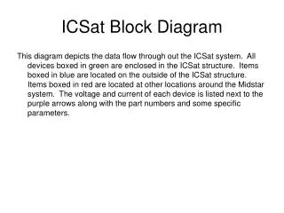
W3207C Block diagram. KC Chien / PNC DDRC Dec. 2005. Confidential. Main board function block. DDR. DDR. NTX2003. K4D551638F-LC40 (4M x 16Bit x 4 Banks 32Mbytes). CH. decoder. Tuner A+DTD13360. PNX8550. D IF. FLASH. DV1. TC58DVM82F1TGI0 (16M x 16BITS 32Mbytes). PNX3000.

W3207C Block diagram
E N D
Presentation Transcript
W3207C Block diagram KC Chien / PNC DDRC Dec. 2005 Confidential
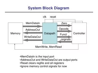
Main board function block DDR DDR NTX2003 K4D551638F-LC40 (4M x 16Bit x 4 Banks 32Mbytes) CH. decoder Tuner A+DTD13360 PNX8550 D IF FLASH DV1 TC58DVM82F1TGI0 (16M x 16BITS 32Mbytes) PNX3000 A IF PNX8550 MIPS32@250 MHz Pixel OSD, TV Control MBS, AC3, Audio delay PNX3000 IF, Switch, ADC Analog audio/video YCX2, CVBSX2,L/R X7, PCaudio CVBS out L/R out USB SPI M25P05 512K bits I2S X5 R,G,B Y/Pb/PrX2 VGA/DVI DV1 DV2 DV3 Tunnel Bus PNX2017 DDR L/R X2 K4D261638F-LC40 (2M x 16Bit x 4 Banks 16Mbytes) PNX2017 Standby uP Color Decoder MBS 3D COMB Audio decoder Audio processor VBI Panel Dlink 1,2,3 Digital Base band Audio/Video Digital 2nd sound IF AVP1 LVDS TDA9975A Audio AMP HDMI X1 SPDIF DV4,DV5 2
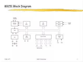
Back (Bottom) DVI optional AV2 AV4 VGA Service port RS232 +USB L/R HDMI PC audio Tuner AV1 AV3 AV out 3
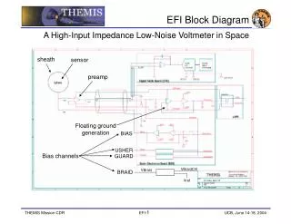
Side AV YC L R CVBS HP 4