Download
1 / 58
630 likes | 1.29k Views
Chapter 7 Operational-Amplifier and its Applications. Outline. Introduction The 741 Op-Amp Circuit The ideal Op Amp The inverting configuration The noninverting configuration Integrator and differentiator The antoniou Inductance-simulation Circuit The Op Amp-RC Resonator

E N D
Chapter 7Operational-Amplifier and its Applications SJTU Zhou Lingling
Outline • Introduction • The 741 Op-Amp Circuit • The ideal Op Amp • The inverting configuration • The noninverting configuration • Integrator and differentiator • The antoniou Inductance-simulation Circuit • The Op Amp-RC Resonator • Bistable Circuit • Application of the bistable circuit as a comparator SJTU Zhou Lingling
Introduction • Analog ICs include operational amplifiers, analog multipliers, A/D converters, D/A converters, PLL, etc. • A complete op amp is realized by combining analog circuit building blocks. • The bipolar op-amp has the general purpose variety and is designed to fit a wide range of specifications. • The terminal characteristics is nearly ideal. SJTU Zhou Lingling
The 741 Op-Amp Circuit • General description • The input stage • The intermediate stage • The output stage • The biasing circuits • Device parameters SJTU Zhou Lingling
General Description • 24 transistors, few resistors and only one capacitor • Two power supplies • Short-circuit protection SJTU Zhou Lingling
The Input Stage • The input stage consists of transistors Q1 through Q7. • Q1-Q4 is the differential version of CC and CB configuration. • High input resistance. • Current source (Q5-Q7) is the active load of input stage. It not only provides a high-resistance load but also converts the signal from differential to single-ended form with no loss in gain or common-mode rejection. SJTU Zhou Lingling
The Intermediate Stage • The intermediate stage is composed of Q16, Q17 and Q13B. • Common-collector configuration for Q16 gives this stage a high input resistance as well as reduces the load effect on the input stage. • Common-emitter configuration for Q17 provides high voltage gain because of the active load Q13B. • Capacitor Cc introduces the miller compensation to insure that the op amp has a very high unit-gain frequency. SJTU Zhou Lingling
The Output Stage • The output stage is the efficient circuit called class AB output stage. • Voltage source composed of Q18 and Q19 supplies the DC voltage for Q14 and Q20 in order to reduce the cross-over distortion. • Q23 is the CC configuration to reduce the load effect on intermediate stage. • Short-circuit protection circuitry • Forward protection is implemented by R6 and Q15. • Reverse protection is implemented by R7, Q21, current source(Q24, Q22) and intermediate stage. SJTU Zhou Lingling
The Output Stage (a) The emitter follower is a class A output stage. (b) Class B output stage. SJTU Zhou Lingling
The Output Stage • Wave of a class B output stage fed with an input sinusoid. • Positive and negative cycles are unable to connect perfectly due to the turn-on voltage of the transistors. • This wave form has the nonlinear distortion called crossover distortion. • To reduce the crossover distortion can be implemented by supplying the constant DC voltage at the base terminals. SJTU Zhou Lingling
The Output Stage • QN and QP provides the voltage drop which equals to the summer of turn-on voltages of QN and QP. • This circuit is call Class AB output stage. SJTU Zhou Lingling
The Biasing Circuits • Reference current is generated by Q12, Q11 and R5. • Wilder current provides biasing current in the order of μA. • Double-collector transistor is similar to the two-output current mirror. Q13B provides biasing current for intermediate stage, Q13A for output stage. • Q5, Q6 and Q7 is composed of the current source to be an active load for input stage. SJTU Zhou Lingling
Device Parameters • For npn transistors: • For pnp transistors: • Nonstandard devices: Q14 and Q20 each has an area three times that of a standard device. SJTU Zhou Lingling
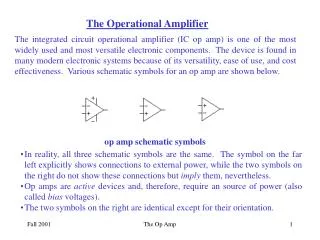
The Ideal Op Amplifier symbol for the op amp SJTU Zhou Lingling
The Ideal Op Amplifier The op amp shown connected to dc power supplies. SJTU Zhou Lingling
Characteristics of the Ideal Op Amplifier • Differential input resistance is infinite. • Differential voltage gain is infinite. • CMRR is infinite. • Bandwidth is infinite. • Output resistance is zero. • Offset voltage and current is zero. • No difference voltage between inverting and noninverting terminals. • No input currents. SJTU Zhou Lingling
Equivalent Circuit of the Ideal Op Amp SJTU Zhou Lingling
The Inverting Configuration • The inverting closed-loop configuration. • Virtual ground. SJTU Zhou Lingling
The Inverting Configuration SJTU Zhou Lingling
The Inverting Configuration SJTU Zhou Lingling
The Inverting Configuration • Shunt-shunt negative feedback • Closed-loop gain depends entirely on passive components and is independent of the op amplifier. • Engineer can make the closed-loop gain as accurate as he wants as long as the passive components are accurate. SJTU Zhou Lingling
The Noninverting Configuration • The noninverting configuration. • Series-shunt negative feedback. SJTU Zhou Lingling
The Noninverting Configuration SJTU Zhou Lingling
The Voltage follower • The unity-gain buffer or follower amplifier. • Its equivalent circuit model. SJTU Zhou Lingling
The Weighted Summer SJTU Zhou Lingling
The Weighted Summer SJTU Zhou Lingling
A Single Op-Amp Difference Amplifier Linear amplifier. Theorem of linear Superposition. SJTU Zhou Lingling
A Single Op-Amp Difference Amplifier • Application of superposition • Inverting configuration SJTU Zhou Lingling
A Single Op-Amp Difference Amplifier Application of superposition. Noninverting configuration. SJTU Zhou Lingling
Integrators The inverting configuration with general impedances in the feedback and the feed-in paths. SJTU Zhou Lingling
The Inverting Integrators The Miller or inverting integrator. SJTU Zhou Lingling
Frequency Response of the integrator SJTU Zhou Lingling
The op-amp Differentiator SJTU Zhou Lingling
The op-amp Differentiator Frequency response of a differentiator with a time-constant CR. SJTU Zhou Lingling
The Antoniou Inductance-Simulation Circuit SJTU Zhou Lingling
The Antoniou Inductance-Simulation Circuit SJTU Zhou Lingling
The Op amp-RC Resonator An LCR second order resonator. SJTU Zhou Lingling
The Op amp-RC Resonator An op amp–RC resonator obtained by replacing the inductor L in the LCR resonator of a simulated inductance realized by the Antoniou circuit. SJTU Zhou Lingling
The Op amp-RC Resonator Implementation of the buffer amplifier K. SJTU Zhou Lingling
The Op amp-RC Resonator • Pole frequency • Pole Q factor SJTU Zhou Lingling
Bistable Circuit • The output signal only has two states: positive saturation(L+) and negative saturation(L-). • The circuit can remain in either state indefinitely and move to the other state only when appropriate triggered. • A positive feedback loop capable of bistable operation. SJTU Zhou Lingling
Bistable Circuit • The bistable circuit (positive feedback loop) • The negative input terminal of the op amp connected to an input signal vI. SJTU Zhou Lingling
Bistable Circuit • The transfer characteristic of the circuit in (a) for increasing vI. • Positive saturation L+ and negative saturation L- SJTU Zhou Lingling
Bistable Circuit The transfer characteristic for decreasing vI. SJTU Zhou Lingling
Bistable Circuit The complete transfer characteristics. SJTU Zhou Lingling
A Bistable Circuit with Noninverting Transfer Characteristics SJTU Zhou Lingling
A Bistable Circuit with Noninverting Transfer Characteristics The transfer characteristic is noninverting. SJTU Zhou Lingling
Application of Bistable Circuit as a Comparator • Comparator is an analog-circuit building block used in a variety applications. • To detect the level of an input signal relative to a preset threshold value. • To design A/D converter. • Include single threshold value and two threshold values. • Hysteresis comparator can reject the interference. SJTU Zhou Lingling
Application of Bistable Circuit as a Comparator • Block diagram representation and transfer characteristic for a comparator having a reference, or threshold, voltage VR. • Comparator characteristic with hysteresis. SJTU Zhou Lingling