Download
1 / 74
740 likes | 1.09k Views
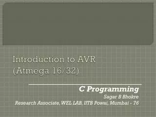
Introduction to AVR ( Atmega 16/32). C Programming Sagar B Bhokre Research Associate, WEL LAB, IITB Powai, Mumbai - 76. Note.

E N D
Introduction to AVR (Atmega 16/32) C Programming Sagar B Bhokre Research Associate, WEL LAB, IITB Powai, Mumbai - 76
Note The assembly language codes mentioned in these slides are just for understanding, most of the aspects will be handled by the C program. However ensuring the working (is handled by C) is left up to the programmer. Sagar B Bhokre
Microcontrollers A microcontroller interfaces to external devices with a minimum of external components Sagar B Bhokre
AVR General Features • The architecture of AVR makes it possible to use the storage area for constant data as well as instructions. • Instructions are 16 or 32-bits • Most are 16-bits and are executed in a single clock cycle. • Each instruction contains an opcode • Opcodes generally are located in the initial bits of an instruction Sagar B Bhokre
AVR Architecture Sagar B Bhokre
AVR General Features Sagar B Bhokre RISC architecture with mostly fixed-length instruction, load-store memory access and 32 general-purpose registers. A two-stage instruction pipeline that speeds up execution Majority of instructions take one clock cycle Up to 16-MHz clock operation
AVR General Features • The ATMega16 can use an internal or external clock signal • Clock signals are usually generated by an RC oscillator or a crystal • The internal clock is an RC oscillator programmable to 1, 2, 4, or 8 MHz • An external clock signal (crystal controlled) can be more precise for time critical applications Sagar B Bhokre
AVR General Features Sagar B Bhokre Up to 12 times performance speedup over conventional CISC controllers. Wide operating voltage from 2.7V to 6.0V Simple architecture offers a small learning curve to the uninitiated.
What is an Interrupt A condition or event that interrupts the normal flow of control in a program Interrupt hardware inserts a function call between instructions to service the interrupt condition When the interrupt handler is finished, the normal program resumes execution Sagar B Bhokre
Interrupt Sources • Interrupts are generally classified as • internal or external • software or hardware • An external interrupt is triggered by a device originating off-chip • An internal interrupt is triggered by an on-chip component Sagar B Bhokre
Interrupt Sources Hardware interrupts occur due to a change in state of some hardware Software interrupts are triggered by the execution of a machine instruction Sagar B Bhokre
Interrupt Handler An interrupt handler (or interrupt service routine) is a function ending with the special return from interrupt instruction (RETI) Interrupt handlers are not explicitly called; their address is placed into the processor's program counter by the interrupt hardware Sagar B Bhokre
AVRInterrupt System • The ATMega16 can respond to 21 different interrupts • Interrupts are numbered by priority from 1 to 21 • The reset interrupt is interrupt number 1 • Each interrupt invokes a handler at a specific address in program memory • The reset handler is located at address $0000 Sagar B Bhokre
Interrupt Vectors • The interrupt handler for interrupt k is located at address 2(k-1) in program memory • Address $0000 is the reset interrupt • Address $0002 is external interrupt 0 • Address $0004 is external interrupt 1 • Because there is room for only one or two instructions, each interrupt handler begins with a jump to another location in program memory where the rest of the code is found • jmp handler is a 32-bit instruction, hence each handler is afforded 2 words of space in this low memory area Sagar B Bhokre
Interrupt Vector Table • The 21 instructions at address $0000 through $0029 comprise the interrupt vector table • These jump instructions vector the processor to the actual service routine code • A long JMP is used so the code can be at any address in program memory • An interrupt handler that does nothing could simply have an RETI instruction in the table • The interrupt vector addresses are defined in the include file Sagar B Bhokre
Interrupt Enabling • Each potential interrupt source can be individually enabled or disabled • The reset interrupt is the one exception; it cannot be disabled • The global interrupt flag must be set (enabled) in SREG, for interrupts to occur • Again, the reset interrupt will occur regardless Sagar B Bhokre
Interrupt Actions • If • global interrupts are enabled • AND a specific interrupt is enabled • AND the interrupt condition is present • Then the interrupt will occur • What actually happens? • At the completion of the current instruction, • the current PC is pushed on the stack • global interrupts are disabled • the proper interrupt vector address is placed in PC Sagar B Bhokre
Return From Interrupt • The RETI instruction will • pop the address from the top of the stack into the PC • set the global interrupt flag, re-enabling interrupts • This causes the next instruction of the previously interrupted program to be executed • At least one instruction will be executed before another interrupt can occur Sagar B Bhokre
Stack Since interrupts require stack access, it is essential that the reset routine initialize the stack before enabling interrupts Interrupt service routines should use the stack for temporary storage so register values can be preserved Sagar B Bhokre
Status Register • Interrupt routines MUST LEAVE the status register unchanged • Optional: Handled by C Program. typical_interrupt_handler: push r0 in r0, SREG … out SREG, r0 pop r0 reti Sagar B Bhokre
Interrupt Variations • AVR Interrupts fall into two classes • Event based interrupts • Triggered by some event; must be cleared by taking some program action • Condition based interrupts • Asserted while some condition is true; cleared automatically when the condition becomes false Sagar B Bhokre
Event-based Interrupts • Even if interrupts are disabled, the corresponding interrupt flag may be set by the associated event • Once set, the flag remains set, and will trigger an interrupt as soon as interrupts are enabled • This type of interrupt flag is cleared • manually by writing a 1 to it • automatically when the interrupt occurs Sagar B Bhokre
Condition-based Interrupts • Even if interrupts are disabled, the interrupt flag will be set when the associated condition is true • If the condition becomes false before interrupts are enabled, the flag will be cleared and the interrupt will be missed • These flags are cleared when the condition becomes false • Some program action may be required to accomplish this Sagar B Bhokre
Sample Interrupts • Event-based • Edge-triggered external interrupts • Timer/counter overflows and output compare • Condition-based • Level triggered external interrupts • USART Data Ready, Receive Complete • EEPROM Ready Sagar B Bhokre
int2 reset int0 int1 External Interrupts • The ATMega16 responds to 4 different external interrupts – signals applied to specific pins • RESET (pin 9) • INT0 (pin 16 – also PD2) • INT1 (pin 17 – also PD3) • INT2 (pin 3 – also PB3) Sagar B Bhokre
External Interrupt Configuration • Condition-based • while level is low • Event-based triggers • level has changed (toggle) • falling (negative) edge (1 to 0 transition) • rising (positive) edge (0 to 1 transition) Sagar B Bhokre
Software Interrupt • If the external interrupt pins are configured as outputs, a program may assert 0 or 1 values on the interrupt pins • This action can trigger interrupts according to the external interrupt settings • Since a program instruction causes the interrupt, this is called a software interrupt Sagar B Bhokre
Timer/Counters The ATMega16 has three timer/counter devices on-chip Each timer/counter has a count register A clock signal can increment or decrement the counter Interrupts can be triggered by counter events Sagar B Bhokre
8-Bit Timer/Counter External Clock Signal Sagar B Bhokre
Timer Events • Overflow • In normal operation, overflow occurs when the count value passes $FF and becomes $00 • Compare Match • Occurs when the count value equals the contents of the output compare register • This can be used for PWM generation Sagar B Bhokre
Output Compare Unit External Output Sagar B Bhokre
Status via Polling • Timer status can be determined through polling • Read the Timer Interrupt Flag Register and check for set bits • The overflow and compare match events set the corresponding bits in TIFR • TOVn and OCFn (n=0, 1, or 2) • Timer 1 has two output compare registers: 1A and 1B • Clear the bits by writing a 1 Sagar B Bhokre
Status via Interrupt • Enable the appropriate interrupts in the Timer Interrupt Mask Register • Each event has a corresponding interrupt enable bit in TIMSK • TOIEn and OCIEn (n = 0, 1, 2) • Again, timer 1 has OCIE1A and OCIE1B • The interrupt vectors are located at OVFnaddr and OCnaddr Sagar B Bhokre
Timer Interrupts • The corresponding interrupt flag is cleared automatically when the interrupt is processed • It may be manually cleared by writing a 1 to the flag bit Sagar B Bhokre
Automatic Timer Actions • The timers (1 and 2 only) can be configured to automatically clear, set, or toggle related output bits when a compare match occurs • This requires no processing time and no interrupt handler – it is a hardware feature • The related OCnx pin must be set as an output; normal port functionality is suspended for these bits • OC0 (PB3) OC2 (PD7) • OC1A (PD5) OC1B (PD4) Sagar B Bhokre
Timer Clock Sources • The timer/counters can use the system clock, or an external clock signal • The system clock can be divided (prescaled) to signal the timers less frequently • Prescaling by 8, 64, 256, 1024 is provided • Timer2 has more choices allowing prescaling of an external clock signal as well as the internal clock Sagar B Bhokre
ATMega16 Prescaler Unit External Clock Signals Sagar B Bhokre
Clock Selection TCCR0 and TCCR1B – Timer/Counter Control Register (counters 0 and 1) CSn2, CSn1, CSn0 (Bits 2:0) are the clock select bits (n = 0 or 1) 000 = Clock disabled; timer is stopped 001 = I/O clock 010 = /8 prescale 011 = /64 prescale 100 = /256 prescale 101 = /1024 prescale 110 = External clock on pin Tn, falling edge trigger 111 = External clock on pin Tn, rising edge trigger TCCR2 – Timer/Counter Control Register (counter 2) CS22, CS21, CS20 (Bits 2:0) are the clock select bits 000 = Clock disabled; timer is stopped 001 = T2 clock source 010 = /8 prescale 011 = /32 prescale 100 = /64 prescale 101 = /128 prescale 110 = /256 prescale 111 = /1024 prescale ASSR (Asynchronous Status Register), bit AS2 sets the clock source to the internal clock (0) or external pin TOSC1) Sagar B Bhokre
Timer/Counter 1 There is only one single byte buffer shared by all of the 16-bit registers in timer 1 • This is a 16 bit timer • Access to its 16-bit registers requires a special technique • Always read the low byte first • This buffers the high byte for a subsequent read • Always write the high byte first • Writing the low byte causes the buffered byte and the low byte to be stored into the internal register Sagar B Bhokre
TCCR1B Timer/Counter 1 Control Register B TCCR1A Timer/Counter 1 Control Register A 7 7 6 6 5 5 4 4 3 3 2 2 1 1 0 0 ICNC1 COM1A1 COM1A0 ICES1 COM1B1 - COM1B0 WGM13 FOC1A WGM12 CS12 FOC1B WGM11 CS11 CS10 WGM10 Timer/Counter 1 Control Register Sagar B Bhokre TCCR1A TCCR1B
Timer 1 Data Registers • TCNT1H:TCNT1L • Timer 1 Count • OCR1AH:OCR1AL • Output Compare value – channel A • OCR1BH:OCR1BL • Output Compare value – channel B • ICR1H:ICR1L • Input Capture Sagar B Bhokre
Switch Bounce Elimination • Pressing/releasing a switch may cause many 0-1 transitions • The bounce effect is usually over within 10 milliseconds • To eliminate the bounce effect, use a timer interrupt to read the switch states only at 10 millisecond intervals • The switch state is stored in a global location to be available to any other part of the program Sagar B Bhokre
Debounce Interrupt .dseg switchstate: .byte 1 .cseg switchread: push r16 in R16, PIND com r16 sts switchstate, r16 pop r16 reti • Global variable holds the most recently accesses switch data from the input port • 1 will mean switch is pressed, 0 means it is not • The interrupt is called every 10 milliseconds • It simply reads the state of the switches, complements it, and stores it for global access Sagar B Bhokre
Timer Setup • Use timer overflow interrupt • Timer will use the prescaler and the internal 8 MHz clock source • Time between counts • 8Mhz/8 = 1 microsec • 8MHz/64 = 8 microsec • 8MHz/256 = 32 microsec • 8MHz/1024 = 128 microsec • The maximum resolutions (256 counts to overflow) using these settings are • /1: 1.000 millisec • /8: 0.512 millisec • /32: 3.125 millisec • /128: 7.812 millisec • Using a suitable prescale, find the required count that should be loaded in the timer. Sagar B Bhokre
Timer Initialization .equ BOTTOM = 100 ldi temp, BOTTOM out TCNT0, temp ldi temp, 1<<TOIE0 out TIMSK, temp ldi temp, 4<<CS00 out TCCR0, temp sei • A constant is used to specify the counter's start value • The Timer Overflow interrupt is enabled • The clock source is set to use the divide by x prescaler • Global interrupts are enabled Sagar B Bhokre
Interrupt Task • On each interrupt, we must reload the count value so the next interrupt will occur in 10 milliseconds • We must also preserve the status register and registers used • The interrupt will alter one memory location • .dseg • ;debounced PIND values • switchstate: .byte 1 Sagar B Bhokre
Interrupt Routine switchread: push temp ldi temp, BOTTOM out TCNT0, temp …switch processing details pop temp reti • The counter has just overflowed (count is 0 or close to 0) • We need to set the count back to our BOTTOM value to get the proper delay • Remember to save registers and status flags as required Sagar B Bhokre
Application lds temp, switchstate ;1 in bit n means ; switch n is down cpi temp, $00 breq no_press …process the switches no_press: … • The application accesses the switch states from SRAM • This byte is updated ever 10 milliseconds by the timer interrupt .dseg switchstate: .byte 1 Sagar B Bhokre
USART Interrupts • Interrupt driven receive and transmit routines free the application from polling the status of the USART • Bytes to be transmitted are queued by the application; dequeued and transmitted by the UDRE interrupt • Received bytes are enqueued by the RXC interrupt; dequeued by the application Sagar B Bhokre
Cautions • The queues are implemented in SRAM • They are shared by application and interrupt • It is likely that there will be critical sections where changes should not be interrupted! ;A queue storage area .dseg queuecontents .byte MAX_Q_SIZE front .byte 1 back .byte 1 size .byte 1 Sagar B Bhokre