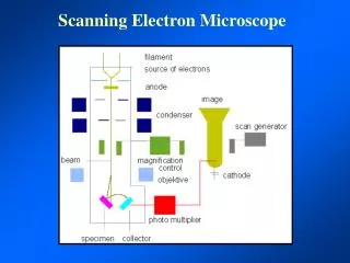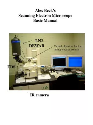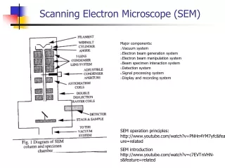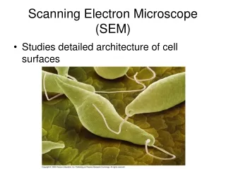
Scanning Electron Microscope
Scanning Electron Microscope. An introduction video: http://virtual.itg.uiuc.edu/training/EM_tutorial/. A short history. TEM constructed in 1931 Von Ardenne first STEM in 1938 by rastering the electron beam in a TEM Zworykin et al. 1942, first SEM for bulk samples

Scanning Electron Microscope
E N D
Presentation Transcript
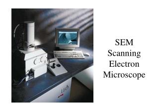
Scanning Electron Microscope An introduction video: http://virtual.itg.uiuc.edu/training/EM_tutorial/
A short history • TEM constructed in 1931 • Von Ardenne first STEM in 1938 by rastering the electron beam in a TEM • Zworykin et al. 1942, first SEM for bulk samples • 1965 first commercial SEM by Cambridge Scientific Instruments Resolution at that time ~ 50 nm <-> Today < 1 nm Morphology only at that time <-> Today analytical instrument
Principles of SEM Magnification? Resolution?
Cathode Ray Tube(CRT) accelerates electrons towards the phosphor coated screen where they produce flashes of light upon hitting the phosphor. Deflection coils create a scan pattern forming an image in a point by point manner
The objective lens aperture Aperture in SEM: either to limit the amount of electrons or enhance contrast
Resolution Can increase the resolution by: How these changes affect the depth of field?
LEO Gemini Column A detector placed within the column is known as an “in-lens” detector and produces a very different image compared to a conventionally located detector
Secondary Electron Detector Side Mounted In-Lens
Secondary Electron Detector In-Lens Side Mounted
Beam deceleration FEI Magellan™ extreme-high-resolution (XHR) SEM
STEM in SEM Oliver Guise et al.
E-beam lithography • High resolution (defined by the beam) • No mask requirement (diverse patterns designed by software) • A variety of resists for choice • Slow compare to photolithography