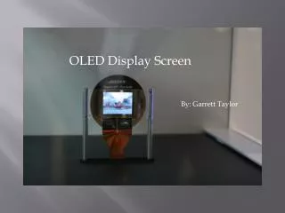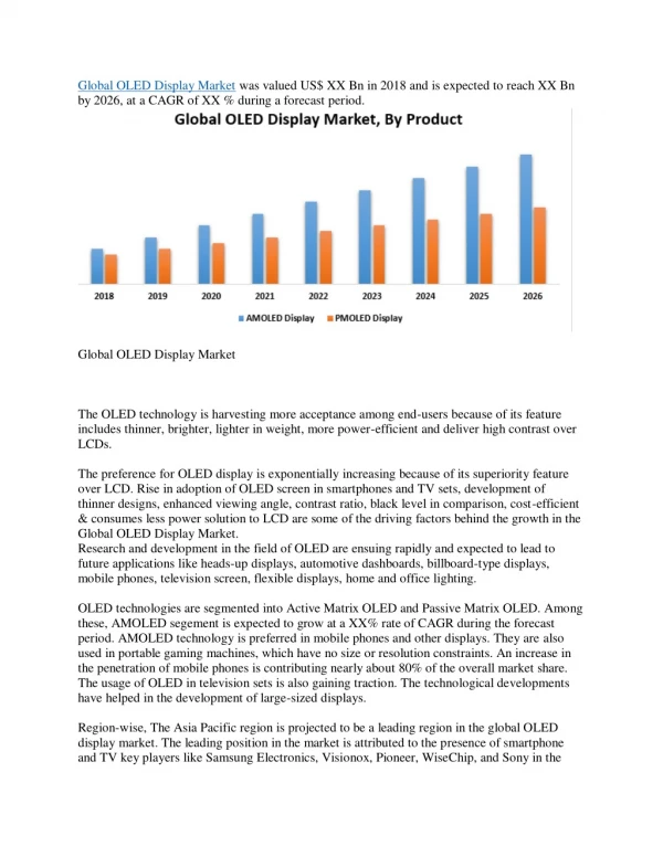
OLED Fabrication
OLED Fabrication. Nesibe Lakhani EECS 277A Prof. Richard Nelson. OLED Structure. OLEDs are light emitting devices that have a thin film of organic compounds as its emissive electroluminescent layer. . Fabrication Methods. Physical Vapor Deposition Screen Printing Ink Jet Printing

OLED Fabrication
E N D
Presentation Transcript
OLED Fabrication NesibeLakhani EECS 277A Prof. Richard Nelson
OLED Structure • OLEDs are light emitting devices that have a thin film of organic compounds as its emissive electroluminescent layer.
Fabrication Methods • Physical Vapor Deposition • Screen Printing • Ink Jet Printing • In-line Fabrication
Physical Vapor Deposition • Thermal vapor evaporation of small molecules occurs in environment of 10e(-6) Torr or higher • It is usually carried out on glass substrate • Multicolor displays are made using properly matched shadow masks for depositing RGB emitting materials
Advantages of PVD • Thickness can be easily controlled • 2-dimensional combinatorial arrays of OLEDs can be easily fabricated in a single deposition procedure • PVD uses the generally available vacuum equipment that exists in the semiconductor industry
Disadvantages of PVD • Expensive • Not flexible • Has no control to direct the materials to deposit on the desired areas • Inefficient use of materials
Screen Printing • Used in low information content displays such as logos and signs • Thin films achieved • Elements of screen printing: screen, stencil, squeegee, ink, press bed, and substrate • Mesh materials can vary from polyester to stainless steel
Screen Printing Steps • The mesh material is stretched across a frame • Hole transport layer prepared using a solution of diamine, polycarbonate, and rubrene. • Squeegee is used to wipe solution through the open mesh • Resulting film covers entire surface of ITO • Electron transport layer (ETL) and cathode aredeposited by PVD
Screen Printing • For patterned hole transport layer (HTL) devices: cathode is deposited in a block larger than the HTL pattern • For non-patterned HTL: cathode is deposited through a mask to create emitting regions of known area for device output measurement
Advantages of Screen Printing • Simple • Lower cost • Great reduction in materials usage because materials are only directed to the printed areas • Faster than inkjet printing • More versatile
Ink Jet Printing • OLEDs are sprayed onto substrates like ink sprayed on paper during printing • Advantages: • Reduced cost • Allows OLEDs to be printed on very large films
Ink Jet Printing Ink jet printing to define and pattern RGB emitting subpixels
In-Line Fabrication • Mass production technique • Vertical in-line tool operates with continuous substrate flow • Linear sources of depositing organic and metallic materials
In-Line Fabrication • Cheaper mass production technique • Excellent thickness homogeneity • Excellent deposition stability • Complicated stack structures possible • High deposition rates/high throughput • High material usage • Large substrate handling
References • Ghassan E. Jabbour et al., Screen Printing for the Fabrication of Organic Light-Emitting Devices, IEEE 7:5, 2001 • Joseph Shinar, Organic Light-emitting Devices. • http://www.ewh.ieee.org/soc/cpmt/presentations/cpmt0401a.pdf • http://www.opera2015.org/deliverables/MONA_CD-ROM/4_Symposium%20Presentations/04-scholles2752.pdf • Muhamad Mat Salleh, et.al., Fabrication of Organic Light Emitting Diodes. • http://optics.org/cws/article/research/24299