Download
1 / 1
10 likes | 238 Views
Bias Modulated Scanning Ion Conductance Microscopy David Perry a,b , Kim KcKelvey b , Sophie Kinnear b , Dmitry Momotenko b , Joshua Byers b and Patrick Unwin b a) MOAC DTC b) Department of Chemistry, University of Warwick, Gibbet Hill Road, Coventry, Warwickshire. Introduction

E N D
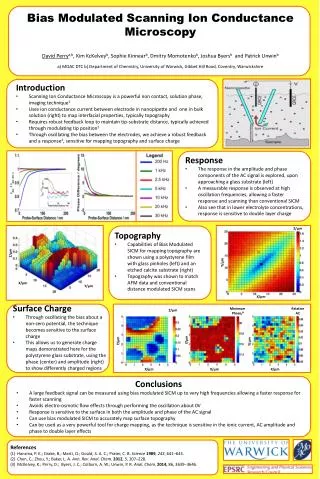
Bias Modulated Scanning Ion Conductance Microscopy David Perrya,b, Kim KcKelveyb, Sophie Kinnearb, Dmitry Momotenkob, Joshua Byersb and Patrick Unwinb a) MOAC DTC b) Department of Chemistry, University of Warwick, Gibbet Hill Road, Coventry, Warwickshire • Introduction • Scanning Ion Conductance Microscopy is a powerful non contact, solution phase, imaging technique1 • Uses ion conductance current between electrode in nanopipette and one in bulk solution (right) to map interfacial properties, typically topography • Requires robust feedback loop to maintain tip-substrate distance, typically achieved through modulating tip position2 • Through oscillating the bias between the electrodes, we achieve a robust feedback and a response3, sensitive for mapping topography and surface charge • Response • The response in the amplitude and phase components of the AC signal is explored, upon approaching a glass substrate (left) • A measurable response is observed at high oscillation frequencies, allowing a faster response and scanning than conventional SICM • Also see that in lower electrolyte concentrations, response is sensitive to double layer charge Z/μm • Topography • Capabilities of Bias Modulated SICM for mapping topography are shown using a polystyrene film with glass pinholes (left) and an etched calcite substrate (right) • Topography was shown to match AFM data and conventional distance modulated SICM scans Z/μm Y/μm X/μm Y/μm X/μm • Surface Charge • Through oscillating the bias about a non-zero potential, the technique becomes sensitive to the surface charge • This allows us to generate charge maps demonstrated here for the polystyrene glass substrate, using the phase (center) and amplitude (right)to show differently charged regions Minimum Phase/° Relative AC Z/μm Y/μm Y/μm Y/μm X/μm X/μm X/μm • Conclusions • A large feedback signal can be measured using bias modulated SICM up to very high frequencies allowing a faster response for faster scanning • Avoids electro-osmotic flow effects through performing the oscillation about 0V • Response is sensitive to the surface in both the amplitude and phase of the AC signal • Can use bias modulated SICM to accurately map surface topography • Can be used as a very powerful tool for charge mapping, as the technique is sensitive in the ionic current, AC amplitude and phase to double layer effects References Hansma, P. K.; Drake, B.; Marti, O.; Gould, S. A. C.; Prater, C. B. Science1989, 243, 641–643. Chen, C.; Zhou, Y.; Baker, L. A. Ann. Rev. Anal. Chem.2012, 5, 207–228. McKelvey, K.; Perry, D.; Byers, J. C.; Colburn, A. W.; Unwin, P. R. Anal. Chem, 2014, 86, 3639−3646.