
Overview
Superconducting Single Photon Nanowire Detectors Development for IR and THz applications. L08. I. Milostnaya, A. Korneev, M. Tarkhov, A. Divochiy, O. Minaeva, V. Seleznev, N. Kaurova, B. Voronov, O. Okunev, G. Chulkova, K. Smirnov, and G. Gol’tsman

Overview
E N D
Presentation Transcript
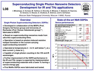
Superconducting Single Photon Nanowire Detectors Development for IR and THz applications L08 I. Milostnaya, A. Korneev, M. Tarkhov, A. Divochiy, O. Minaeva, V. Seleznev, N. Kaurova, B. Voronov, O. Okunev, G. Chulkova, K. Smirnov, and G. Gol’tsman Moscow State Pedagogical University, Moscow 119992, Russia MSPU Overview State-of-the-art NbN SSPDs Device performances Single Photon Superconducting Detectors (SSPDs) • Developed in collaboration of the MSPU (Prof. Gregory Gol’tsman group) and University of Rochester (Prof. Roman Sobolewski group)1-4, fabricated at MSPU • Based on superconducting nanowires made from ultra-thin superconducting films. • Operation is based on photon-induced resistive hotspot formation in the current-carrying superconducting nanowire2. • Operated at temperatures 2 - 4.2 Kwell below Tc at a bias current Ib close to Ic. • Capable of single photon counting in the VIS and IR waveranges. • Further improvement of the SSPD performance in the IR and THz ranges is expected by implementation of superconducting materials with a lower Tc having a narrow energy gap. • First MoRe SSPDs were fabricated and tested.
SSPDs Fabrication at MSPU The mature technology is developed for NbN SSPDs. • NbN films properties: • Thickness 4 nm • Critical temperature Tc=10-11K • Transition width Δ Tc=0.3K • Critical current density jc=7x10⁶ A/cm2 • Deposition of 4-nm-thick NbN film on Sapphire substrate by DC magnetron sputtering of Nb target in in Ar+N2 mixture • Patterning of stripe windows by direct e-beam lithography • Formation of Au contacts by optical lithography • Formation of meander-shaped structure with reactive ion etching ’Standard’ Device Design Advanced SSPD Design • SSPDs are designed as meander-shaped nanowires connected to Au contact pads intended for connection to a coplanar waveguide. • Multisection SSPDs with lower kinetic inductance are designed as several meander nanowires connected in parallel • Subnanosecond photoresponse time achieved • Meander size • 10x10μm2 • Nanowire width • 80 - 100 nm • Linepitch • 200 nm • Nanowire length • up to 500 μm SEM image of the 10 mm x 10 mm SSPD Spectral dependence of QE for a NbN SSPD at 3K and 5K at bias current of 0.94 Ic. • Drawback: response time is significantly affected by ananowire kinetic inductance. Response of a single 500-µm-long nanowire Oscillograms of the response for 2-section (a) and 5-section (b) SSPDs
MoRe SSPD • Motivation. The use of a material with the narrow energy gap and low quasiparticles diffusivity should shift the detectors sensitivity towards longer wavelengths. • Technology of ultra-thin MoRe films suitable for SSPD was developed. Ultrathin (4-10 nm thick) MoRe films were deposited by DC magnetron sputtering of a Mo60/Re40target. Best MoRe films properties: Thickness 4 nm 10 nm Critical temperature Tc=7.7 K 9.7K Transition width Δ Tc=0.1K 0.2K Critical current density at 4.2K jc=1.1x10⁶ A/cm2 Sheet resistance Rs=65-75 /□ • ‘Standard’ SSPD nanowire meander structures of good quality were fabricated and tested. • First single-photon response was obtained for 1.26mm photons at operational temperature of 4.2K. Oscillogram of the single-photon response of a 200-nm-wide MoRe nanowire Dependence of a counting rate on a bias current
References [1]G. Gol'tsman at al., Appl. Phys. Lett. 79 (2001), 705. [2] A. Semenov at al., Physica C, 352 (2001), 349. [3] G. Gol’tsman et al.,IEEE Trans. on Appl. Supercond. 13(2) (2003), 192. [4] A. Korneev et al., Appl. Phys. Lett. 84 (2004), 5338. [5] A. Korneev et al., SPIE Europe Int. Congress on Optics and Optoelectronics, Prague, Czech Republic, 16 - 19 April 2007.


