Download
1 / 5
50 likes | 60 Views
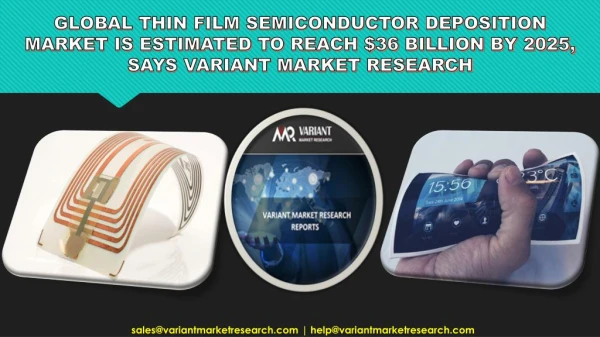
VacuumLtd is one of the world's best thin film deposition system manufacturing company in Dubai, UAE. It also manufactures other products such as Thin film deposition, Thin film deposition system, VST, PVD thin film deposition system, Evaporation, Evaporation System, E-beam Evaporation, Thermal Evaporation, Sputtering System, CVD Thin film deposition.<br>For more info visit our site : https://vacuumltd.com/<br>

E N D
World’s Best Thin Film Deposition System Available in Dubai, UAE, and Israel
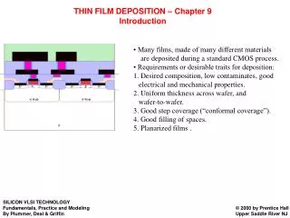
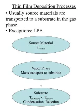
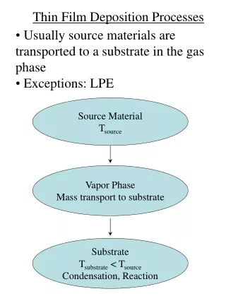
In the industrial sector, one of the process technologies used to create electrical circuits is called thin film deposition. This system usually consists of a chamber in which the substrate is placed, and a number of sources that supply the material to be deposited. The sources are typically located around the perimeter of the chamber, and the deposited material is typically deposited onto the substrate in a circular motion. This process is used to create thin film solar cells, integrated circuits (ICs), and other optoelectronic devices .
One of the benefits of using a Thin film deposition systemis that it can be used to create very intricate patterns and shapes that would be difficult or impossible to create using other methods. Additionally, thin film deposition systems are relatively low-cost and have a high degree of control over the properties of the deposited material. VST is providing the world’s best thin film deposition system and is now available in Dubai, UAE, and Israel
Types of Thin film deposition: There are three types of thin film deposition systems: physical vapor deposition, chemical vapor deposition, and Plasma-Enhanced Chemical Vapor Deposition (PE-CVD). 1.(PVD Thin Film Deposition System):Physical vapor deposition(PVD) is a high-energy technique that vaporizes solid materials in a vacuum for deposition onto a target material. Two methods of PVD include evaporation and sputtering. 1.1 Evaporation:Evaporation system is the most common type of thin film deposition. In this process, a material is heated until it becomes a vapor and then deposited onto a substrate. Furthermore, it is divided into two types, E-beam evaporation, and thermal evaporation. 1.1.1 E-beam Evaporation: E-beam evaporation uses a high-energy electron beam evaporator to evaporate the material. This vapor then creates a thin film for deposition. This method is commonly used for solar panels and glass.
1.1.2 Thermal Evaporation: Thermal evaporation is a simple form of physical vapor deposition. This method creates a reaction through extreme heat to vaporize the target material. Thermal evaporation is useful for creating OLEDS and thin-film transistors. 1.2 Sputtering: Sputtering system is another common thin film deposition method. It is often called a billiard game on the atomic scale. In this process, the erosion of the metal by bombardment with energetic ions happens. The ions may be generated by ion beam sputtering or in a low-pressure plasma. They hit the surface of a target metal and cause the ejection of atoms by momentum transfer in a collision. 2. CVD Thin Film Deposition:Chemical vapor deposition(CVD) is a process in which a solid film is deposited on a substrate by reacting gases in a chemical reaction. CVD is used to create films with high purity, good dimensional control, and good adhesion to the substrate. However, CVD reactions can be difficult to control, making the process less suited for large-scale production. This method can be used to deposit materials such as metals, alloys, oxides, and semiconductors. 3. Plasma-enhanced CVD Thin Film Deposition: Plasma-enhanced chemical vapor deposition is a process in which plasma is used to assist in the reaction of gases to deposit a film onto a substrate. PE-CVD can be used to create films with high purity, good adhesion, and good electrical properties. However, PE-CVD reactions can be difficult to control, making the process less suited for large-scale production.