Download
1 / 77
770 likes | 1.22k Views
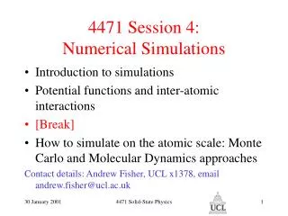
Summary of 4471 Session 5: Simulations and Surfaces. More on numerical simulation techniques: Extracting information from Monte Carlo calculations (e.g. energy, heat capacity, free energy) Comparison of molecular dynamics and Monte Carlo methods

E N D
Summary of 4471 Session 5:Simulations and Surfaces More on numerical simulation techniques: • Extracting information from Monte Carlo calculations (e.g. energy, heat capacity, free energy) • Comparison of molecular dynamics and Monte Carlo methods • Interatomic interactions beyond the pair potential • Structure of (crystalline, clean) surfaces: • Two-dimensional crystallography • Low Energy Electron Diffraction (LEED) • The silicon (001) surface as an example of a surface reconstruction driven by local bonding changes 4471 Solid-State Physics
4471 Session 7: Nanotechnology • A survey of possibilities for nanotechnology • Ways of making and characterising nanoscale structures • Lithography (conventional, electron-beam, ‘soft’) • Scanning probe microscopy • Self-assembly and directed assembly • Some electronic properties of nanoscale systems • Coulomb blockade • Conductance quantization 4471 Solid-State Physics
Richard Feynman’s 1959 Lecture • Richard Feynman at the 1959 annual meeting of the American Physical Society: But I am not afraid to consider the final question as to whether, ultimately---in the great future---we can arrange the atoms the way we want; the very atoms, all the way down! What would happen if we could arrange the atoms one by one the way we want them…? 4471 Solid-State Physics
What is Nanotechnology? • A set of tools and ideas for the manipulation and control of matter in the size range between 0.1nmand 1m • Corresponds to the range of sizes between current electronics and atomic/molecular dimensions 4471 Solid-State Physics
Possible applications in electronics • Current CMOS electronic technology may be approaching fundamental limits in hardware performance and cost • New types of electronic components (e.g. wires, transistors) operating at smaller length scales • Completely new ways of manipulating information (e.g. using reorientable magnetisation of small magnetic particles) • New ways of coupling light to electronic processes (e.g. using patterns on the scale of the optical wavelength) 4471 Solid-State Physics
Possible applications in biomedicine • Understanding of the function of biomolecules - particularly the cooperation between them, and their function in cell membranes (difficult to study by conventional crystallography) • Controlling interaction of cells with their environment (e.g. tissue culture, biocompatibility of implants) 4471 Solid-State Physics
Richard Feynman’s 1959 Lecture • Richard Feynman at the 1959 annual meeting of the American Physical Society: Another thing we will notice is that, if we go down far enough, all of our devices can be mass produced so that they are absolutely perfect copies of one another. We cannot build two large machines so that the dimensions are exactly the same. But if your machine is only 100 atoms high, you only have to get it correct to one-half of one percent to make sure the other machine is exactly the same size---namely, 100 atoms high! 4471 Solid-State Physics
Methods for producing structure on the nanoscale • How do we pattern matter on the nanometer lengthscale? • Using layer-by-layer growth • By interaction with a ‘beam’ of light or particles • By interaction with a scanning probe tip • By using contact with a ‘stamp’ or ‘mask’ • By exploiting molecules’ natural tendency to order as a result of their mutual interactions 4471 Solid-State Physics
Optical or UV lithography • Standard method for current generation semiconductor device processing (CMOS) • Use a ‘resist’ whose susceptibility to etching is affected by light • Resolution depends on wavelength of light used: current (2001) standards for fabrication 0.15m Activated resist Chemical etch (e.g. HF) 4471 Solid-State Physics
Electron beam lithography • Just as have higher spatial resolution in imaging with shorter-wavelength electron microscopes, have higher resolution in patterning too • Sensitive to electrons because can induce free radical formation (promoting resist removal) or crosslinking (preventing resist removal) 4471 Solid-State Physics
Electron beam lithography • Possible to produce feature sizes down to about 5nm using this technique • Figure shows 5nm metallic line on silicon surface (Welland et al., Cambridge) 4471 Solid-State Physics
Soft lithography - nanoimprint lithography • Can print a structure directly on to a ‘soft’ surface (e.g. a polymer) from a ‘hard’ mould (e.g. a metal surface prepared by e-beam lithography) 4471 Solid-State Physics
Soft lithography - nanoimprint lithography • Get a variety of structures e.g. holes and pillars 4471 Solid-State Physics
Soft lithography - lithographically induced self-assembly (LISA) • Apply a large electric field between a mask and a polymer film • Polymer film spontaneously grows up towards mask: • Pillars form when mask-polymer separation between 200nm and 800nm • Works because polymer attracted to high-field region Mask Polymer film 4471 Solid-State Physics
The scanning probe idea • Get very high spatial resolution by • Scattering very short-wavelength waves Sample 4471 Solid-State Physics
The scanning probe idea • Get very high spatial resolution by • Scattering very short-wavelength waves and detecting them a long way away (e.g. electron microscopy, neutron or X-ray diffraction) Sample 4471 Solid-State Physics
The scanning probe idea • Get very high spatial resolution by • Scattering very short-wavelength waves and detcecting them a long way away (e.g. electron microscopy, neutron or X-ray diffraction) • Bringing a small detector up to the sample Sample 4471 Solid-State Physics
The scanning probe idea • Get very high spatial resolution by • Scattering very short-wavelength waves and detcecting them a long way away (e.g. electron microscopy, neutron or X-ray diffraction) • Bringing a small detector up to the sample and arranging for a very localised interaction between them Sample 4471 Solid-State Physics
The scanning probe idea • Get very high spatial resolution by • Scattering very short-wavelength waves and detcecting them a long way away (e.g. electron microscopy, neutron or X-ray diffraction) • Bringing a small detector up to the sample and arranging for a very localised interaction between them Scan detector across sample Sample 4471 Solid-State Physics
The STM(Scanning Tunnelling Microscope) • Electrons tunnel across small (few Å) vacuum gap between tip and sample. • Relies on sensitivity of tunnelling to tip-surface distance (hence localised interaction). • Normal mode of operation is ‘constant-current’: feedback loop keeps current constant as tip is scanned across surface. 4471 Solid-State Physics
Tersoff-Hamann Theory • Assume • Tip-sample tunnelling probability small (so ‘perturbation theory’ can be applied); • Spherically symmetric tip; • Initial state for tunnelling is an s state on tip • Fermi’s golden rule for rates in quantum physics then gives conductance: 4471 Solid-State Physics
Tersoff-Hamann Theory (2) • Write the matrix element in terms of the current operator as • Assuming S lies in a region of constant potential, and that we tip wavefunction is an exponentially decaying s-wave, we can do all the integrals to get 4471 Solid-State Physics
What does this mean? • Conductance proportional to probability of finding highest-energy electrons outside the sample near the tip • The STM measures the ‘local density of states’ (under certain conditions) Surface Tip rtip 4471 Solid-State Physics
Atomic manipulation with the STM: the ground state Atom on surface • Can use presence of tip to affect the potential energy of atoms on or near the surface • Allows movement of individual atoms along the surface (‘parallel process’)... Potential energy Distance along surface 4471 Solid-State Physics
Atomic manipulation with the STM: the ground state • Can use presence of tip to affect the potential energy of atoms on or near the surface • Allows movement of individual atoms along the surface (‘parallel process’)... STM tip Potential energy Distance along surface 4471 Solid-State Physics
Atomic manipulation with the STM: the ground state • Can use presence of tip to affect the potential energy of atoms on or near the surface • Allows movement of individual atoms along the surface (‘parallel process’)... Potential energy Distance along surface 4471 Solid-State Physics
Atomic manipulation with the STM: the ground state • Can use presence of tip to affect the potential energy of atoms on or near the surface • Allows movement of individual atoms along the surface (‘parallel process’)... Potential energy Distance along surface 4471 Solid-State Physics
Atomic manipulation with the STM: the ground state • Can use presence of tip to affect the potential energy of atoms on or near the surface • Allows movement of individual atoms along the surface (‘parallel process’)... Potential energy Distance along surface 4471 Solid-State Physics
Atomic manipulation example: Xe atoms on Ni at T=4K • Individual Xe atoms manipulated by the parallel process at T=4K • STM tip moves `up’ over atoms, showing that electrons tunnel more easily through them than through vacuum Don Eigler et al (IBM Almaden) 4471 Solid-State Physics
Atomic manipulation example: Xe atoms on Ni at T=4K • Individual Xe atoms manipulated by the parallel process at T=4K • STM tip moves `up’ over atoms, showing that electrons tunnel more easily through them than through vacuum Don Eigler et al (IBM Almaden) 4471 Solid-State Physics
STM manipulation example: ‘molecular abacus’ • Produced from C60 molecules (about 5Å across) • Can be ‘pushed along’ with the STM tip Jim Gimzewski et al (IBM Zurich) 4471 Solid-State Physics
STM manipulation: use of electronic forces • Can use the electronic state to manipulate atomic positions in various ways • The ‘electron wind effect’ (electrons transfer momentum to atoms) • This is believed to be the physics behind the ‘atomic switch’ (on and off states correspond to atom on tip and on surface) e- e- Atom on surface Surface Force 4471 Solid-State Physics
STM manipulation: use of electronic forces Potential energy • Can also exploit transient change of chemical environment as a tunnelling electron passes through the system • Temporary occupation of antibonding electronic states can lead to desorption of atoms (‘DIET’- desorption induced by electronic transitions) Antibonding state occupied by tunnelling electron Distance from surface Electronic ground state 4471 Solid-State Physics
STM manipulation: use of electronic forces • Example: removal of H atoms from a passivated Si(001) surface • Conducting `line’ of reactive bonds, one atom wide • Behaves like an atomic wire H atoms removed here Hitosugi et al, Tokyo University and Hitachi 4471 Solid-State Physics
Single-molecule vibrations • Study vibrations of individual molecules and individual bonds by looking at phonon emission by tunnelling electrons Wilson Ho et al., UC Irvine 4471 Solid-State Physics
Single-molecule vibrations • Study vibrations of individual molecules and individual bonds by looking at phonon emission by tunnelling electrons • New possibilities for inducing reactions by selectively exciting individual bonds…. Wilson Ho et al., UC Irvine 4471 Solid-State Physics
Scanning Force Microscopy (SFM) • We would like to • be able to image insulating (as well as conducting) surfaces • measure forces, as well as currents, on the atomic scale, in order to • learn more about them • control the manipulation process • The solution: scanning force microscopy (SFM) 4471 Solid-State Physics
Scanning force microscopy • Measure deflection of small ‘cantilever’ on which tip is mounted, by deflection of a laser beam 4471 Solid-State Physics
Scanning force microscopy • It used to be thought that contact mode would give the best resolution, but the interpretation is complicated by strong mechanical interactions between the tip and the sample Alex Shluger et al, CMMP, UCL 4471 Solid-State Physics
Scanning force microscopy • Most recent development is ‘non-contact’ force microscopy: tip vibrates above sample and only approaches briefly 4471 Solid-State Physics
Scanning force microscopy • Allows truly atomic-resolution force microscopy images to be obtained for the first time. Defects on surface Defects ‘migrate’ Ernst Meyer et al, Basel 4471 Solid-State Physics
Scanning force microscopy • Allows truly atomic-resolution force microscopy images to be obtained for the first time. Atomic ‘step’ on surface Ernst Meyer et al, Basel 4471 Solid-State Physics
Scanning force microscopy • Understanding the physics behind the formation of these images is complicated... Image of NaCl ‘island’ Simulated tip scan Ernst Meyer et al, Basel Adam Foster and Alex Shluger, CMMP, UCL 4471 Solid-State Physics
Other ways of producing structure with SPM • Find a local chemical reaction promoted by the presence of a tip - for example oxidation… • …or exposure of a resist (as in e-beam lithography) 4471 Solid-State Physics
Other ways of producing structure with SPM • Find a local chemical reaction promoted by the presence of a tip - for example oxidation… • …or exposure of a resist by the local electron current (as in e-beam lithography) 4471 Solid-State Physics
Self-assembly • Exploit chemical forces to produce organization into desired patterns • Inspired by biology (and soap!): e.g. spontaneous formation of bilayer membranes (living cells and soap films) Hydrophilic headgroups (polar) Hydrophobic tails (non-polar) 4471 Solid-State Physics
Self-assembly • Generate films on metal surfaces by a similar method: end ‘tail’ part of molecule with an S-H group that reacts with gold • Head group can now be arbitrary (e.g. a biological antibody or antigen) Headgroup C-S-Au bonds Gold substrate 4471 Solid-State Physics
Quantum dots and huts • Also get spontaneous self-organization in other ways, for example during ‘strained’ growth of one material on another when their lattice parameters differ 4471 Solid-State Physics
Examples of atomic-scale lines • Lines of Si ad-dimers formed by annealing (heating) the Si-rich SiC(001) surface • Self-assembly, probably mediated by long-range elastic interactions between the lines 4471 Solid-State Physics
Directed growth • Try to combine the idea of control (as in lithography) and spontaneous formation of an ordered structure (as in self-assembly) by ‘directed growth’ that is spontaneous following some initiation event • For example, use an SPM initiation (slow, expensive, can only be done at a limited number of sites) followed by a self-propagating chemical reaction 4471 Solid-State Physics