Download
1 / 17
0 likes | 5 Views
The Journal of Experimental Life Sciences is a peer-reviewed scientific journal dedicated to the exploration and advancement of experimental research in the field of life sciences. The journal provides a platform for publishing high-quality, original research that uses experimental methods to investigate biological processes, systems, and phenomena.<br>

E N D
Journal of Science and Technology ISSN: 2456-5660 Volume 8, Issue 06 (June -2023) www.jst.org.in DOI:https://doi.org/10.46243/jst.2023.v8.i06.pp20 - 36 High Gain Step-Up Dickson Converter with Interleaved Topology for Applications In Renewable Energy Amritha N K, Saneep K Dept. of EEE, NSS College of Engineering, Palakkad, Kerala To Cite this Article Amritha N K, Saneep K, High Gain Step-Up Dickson Converter with Interleaved Topology for Applications In Renewable Energy” Journal of Science and Technology, Vol. 08, Issue 06,-June 2023, pp20-36 Article Info Received: 17-05-2023 Revised: 17-06-2023 Accepted: 23-06-2023 Published: 30-06-2023 Abstract Power electronics become a crucial factor on integrating Renewable Energy Sources more into the main grid. Renewable energy resources make the power converters to have a functional and versatile value. Enhancement of the voltage output from the renewable energy systems to a higher level can be achieved using DC-DC Converters. Several converters topologies have been implemented so far and Dickson converter proves to be a high efficient and high performance converter. The Dickson charge pump along with the Interleaved boost stage provides high voltage gain, reduced current ripples and losses in the components. The converter delivers an output with minimal voltage stresses on passive components and semiconductor devices, which enhances the voltage potential for enhancing the maximum power output requirements. The advanced converter topologies also make the integration with distribution systems more beneficial. This project compares Interleaved Boost Converter, Hybrid Nonisolated DC-DC Converter, Modified Dickson Converter with Voltage Multiplier and Bifold Dickson Converter with Five VMC Stages to understand the voltage stresses of different components in the converter, from which the efficiency analysis is made to decide the better converter among the four. The converters are studied in detail by simulation analysis using MATLAB/SIMULINK. Voltage stress and other parameters of each component are obtained and the performance of converters are evaluated. The study is extended to the comparison of each converters . Hardware prototype of the converter is implemented for the validation and testing of the converter on giving a 24V, 4A supply and obtaining a 400V DC output. DC-DC Converters are becoming popular used now-a-days as the dependence on the renewable energy resources have increased. Unlike the conventional sources including fossil fuels, renewable energy resources are the one which get replenished easily. For the most part, renewable energy sources also provide clean energy, or energy that emits few greenhouse gases or pollutants. The difficulty is achieving the technology, infrastructure, and political support to make this transition. There are different sources available, that Published by: Longman Publishers www.jst.org.in Page | 20
Journal of Science and Technology ISSN: 2456-5660 Volume 8, Issue 06 (June -2023) www.jst.org.in DOI:https://doi.org/10.46243/jst.2023.v8.i06.pp20 - 36 include solar energy, wind energy, hydroelectric energy, geothermal , and so on. On coming to the case of each energy resources, Hydroelectric energy is by far the most prevalent, accounting for 83% of the world's electricity generation from renewable sources. This is most likely because the requisite technology to generate electricity by harnessing the flow of water has been around the longest, dating back to the early 20th century. Wind energy is the next largest, at just over 7% of the electricity generated from renewable sources, followed by biowaste and biomass energy (7%), geothermal energy (2%), and solar, tidal, and wave energy (less than 1%). In many industrial applications, it is required to convert a fixed- voltage dc source into a variable voltage dc source. DC-DC converters are power electronic circuits that convert a dc voltage to a different dc voltage level, often providing a regulated output. DC converters widely used for traction motor in electric automobiles, trolley cars, marine hoists, and forklift trucks. They provide smooth acceleration control, high efficiency, and fast dynamic response. DC converter can be used in regenerative braking of dc motor to return energy bake into the supply, and this feature results in energy saving for transportation system with frequent stop; and also are used, in dc voltage regulation. In renewable energy grid-connected power systems and dc microgrid systems, there are many low voltage power sources, such as solar photovoltaic (PV) modules and fuel cells. Thus, a front-end high step- up dc–dc converter is needed as an interface between the low voltage source and the dc bus. DC conversion is of great importance in many applications, starting from low power applications to high power applications. The goal of any system is to emphasize and achieve the efficiency to meet the system needs and requirements. Several topologies have been developed in this area, but all these topologies can be considered as apart or a combination of the basic topologies which are buck, boost and fly back. For low power levels, linear regulators can provide a very high-quality output voltage. For higher power levels, switching regulators are used. Switching regulators use power electronic semiconductor switches in On and Off states. Because there is a small power loss in those states (low voltage across a switch in the on state, zero current through a switch in the off state), switching regulators can achieve high efficiency energy conversion. The main intention of using DC-DC Converters in power generation applications is to improve the power gain. Several topologies are bought up to increase the voltage level from the energy resources inorder to meet the existing power demands. So for meeting the power demand , conventionally boost converters were employed. Conventional boost converters works with high duty cycle values to obtain a higher output, which itself is a disadvantage. Practically, the gain of the Conventional Boost Converters is limited by the conduction losses, and obtaining a high-voltage-gain ratio is not feasible. Not only that, but the Conventional Boost Converters also suffers from the voltage stress and reverse recovery phenomenon at high voltages and requires a large inductor to operate in the Continuous Conduction Mode.So several modifications were performed in boost converters inorder to obtain a highly efficient output with low losses. The aim was to maintain duty cycle value almost symmetric and reduce the losses of the converter. There are different topologies adopted in Conventional Boost Converter, like, cascaded topologies, which obtain high voltage level with low duty cycles. Due to the cascaded topology, power is processed multiple times so making the control complicated. The three- level boost converter is derived from the series-input series-output multiphase boost converter. The stress on the switches and inductance requirement is reduced. However, it still has the same gain as the Conventional Boost Converter. The single-switch quadratic boost Published by: Longman Publishers www.jst.org.in Page | 21
Journal of Science and Technology ISSN: 2456-5660 Volume 8, Issue 06 (June -2023) www.jst.org.in DOI:https://doi.org/10.46243/jst.2023.v8.i06.pp20 - 36 converter has a simple structure and does not suffer from instability like the cascaded boost converter. However, the voltage and current stress across the switches are high, and the inductor that ensures the CCM operation is large. Another option was to increase the turns ratio of the transformer or coupled inductor. This happens in forward, flyback, or full bridge topologies. These devices suffer from parasitic leakage inductance, which significantly increases the voltage stress on the active switches and can cause damage unless additional auxiliary is used. They are bulky and unfeasible and has large copper losses , leading to efficiency reduction. The leakage inductor of the magnetic coupling element has a problem that cause high voltage spikes in the circuit. Hence, an active or passive clamp is usually adopted to recycle the leakage energy. Moreover, in case of voltage-fed transformer-isolated dc–dc converters, the input current ripple is relatively large, which may seriously increase the losses of the input filter capacitors and degrade the low voltage power sources. efficiency and low cost. Using VMC with conventional boost converters have found to improve the voltage gain and performance. But still inductor size is substantial. Therefore, VMC is used with interleaved boost stage to enhance the input current. By using voltage multiplier units the voltage level get multiplied by the number of the VM stages and output can be levelled up . The voltage and current stress on the internal components depend on the VMC connections and the number of cells. By interleaving , two converters are interconnected so as to have two inductors, which is identical. Interleaving helps in filtering by connecting two or more power stages in parallel , bur driven in different phases. Effectively, it is two boost converters with phase shift connected in parallel. So non isolated DC-DC Converters are opted because of its high power density, high impedance of Cockcroft-Walton VMC increases rapidly as the number of stages increases and reducing the efficiency of the converter. Also, connecting many capacitors in series limits the efficient multiplications to only if the stray capacitances are much smaller than series connected capacitors. On the other hand, the voltage stress across Dickson based VMC increase as the number of the stages increases. Although the modified Dickson VMC has lower voltage stress across the components than the original Dickson cell, it only works for an odd number of VMC. The Cockcroft Walton VMC has equal voltage stress on all capacitors. The output voltage gain ratio to integrate with high voltage DC bus. The voltage stress of the components are low and the input current is shared equally among the two phases, irrespective of the VMC stage number. Hence the conduction losses and thermal losses are reduced. Each stage has two capacitors thereby cancelling the voltage ripple. By the interleaving nature , input current is continuous with low ripple. This would help in accurate current measurement for maximum power point tracking (MPPT). Filter requirements are also reduced. The converter does not require an output diode or an LC filter to regulate the output voltage, so each stage can produce a constant DC voltage. High voltage gain interleaved DC-DC Converter with Dickson topology has high voltage gain with advantages such as ease of on-chip integration, light weight, and high power density, as only capacitors are employed as energy storage elements. The voltage conversion ratios of SC converters can be expanded easily through cascaded multiple SC cell topologies. There are many limitations for the conventional SC converters. In addition, the absence of magnetic components leads to high current spikes in the switching transients, which is suppressed by raising the time constant of parasitic resistance and equivalent capacitance , high capacitance value is required. The input current of these converters has a Switched-capacitor (SC) converters are another attractive solution to achieve a high Published by: Longman Publishers www.jst.org.in Page | 22
Journal of Science and Technology ISSN: 2456-5660 Volume 8, Issue 06 (June -2023) www.jst.org.in DOI:https://doi.org/10.46243/jst.2023.v8.i06.pp20 - 36 pulsating nature, hence having large current ripple and electromagnetic interference troubles, thereby constraining high power level applications. additional small inductors resonate in series with the switched capacitors inorder to achieve zero current switching (ZCS) for the semiconductor devices are proposed. Thus, the switching losses are reduced, and large capacitance values are not needed to suppress the current spikes, so the utilization of the switched capacitors is improved. However, the voltage regulation of such resonant dc– dc converters is still complicated. Hybrid SC topology dc–dc converters combining SC structure and the conventional boost converter have been proposed. By using an input inductor, the PWM voltage regulation and input current continuity can be realized, while the high voltage gain and low voltage stresses of semiconductor devices are maintained. However, the problem of high current spikes still exists in SC network, and the main active switches and diodes in these converters operate in hard switching, leading to considerable switching losses. Different topologies of Hybrid SC converter with Dickson SC structures are present to obtain the soft charging operation which can eliminate the voltage mismatch among the switched capacitors. One among these converter topologies is the combination of interleaved boost converter with Dickson SC Converters. By introducing small resonant inductors into SC networks, zero voltage switching (ZVS) turn-on conditions for all active switches and ZCS turn-off conditions for some of the diodes can be achieved; in addition, the reverse recovery transients for the other diodes are also alleviated by the resonant inductors. Hence current spikes and switching losses are reduced. It includes the features like, PWM Voltage Regulation, high voltage gain and low voltage stress across the semiconductor devices. The interleaving operation increase the power level and also provide low rippled continuous input current. This reduce the size and the losses in the input filter capacitors. SC-based resonant dc-dc converters, in which distributed stray inductances or Principle of Operation The converters mentioned have a interleaved boost stage and a Dickson voltage multiplier stage. Interleaved boost stage has two inductors connected to source, for the boosting operation. It is switched by low side switches. Interleaved stage stores the energy and supply it to the Dickson VMC stage. Dickson converter can have different number of stages each having 2 diodes and 2 capacitors. Dickson converters with number of stages N=2 is similar to Greinacher VMC, but Greinacher is not extensible , but Dickson could be. VM stage helps in upgrading the output level. There is 180 degree phase shift between the gate signals of active switches. In case of interleaved converters duty cycle should not be less than 50%, there is a chance for imbalance in the capacitor voltage and voltage gain reduction. Certain assumptions are taken for the analysis: oAll components are considered to be ideal oLarge capacitor values are taken so as to neglect the voltage ripples oSteady state operation of the converters oDuty cycles are taken to be greater than or equal to 50% oSingle source voltage source is taken as the input Here three converters are taken into consideration. They share a similarity in the operating principle, that, they are Interleaved Boost Converter, and the modifications of IBC, i.e, Bifold Published by: Longman Publishers www.jst.org.in Page | 23
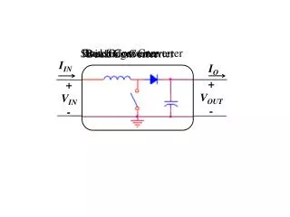
Journal of Science and Technology ISSN: 2456-5660 Volume 8, Issue 06 (June -2023) www.jst.org.in DOI:https://doi.org/10.46243/jst.2023.v8.i06.pp20 - 36 Dickson VMC Converter with five stages, Modified Dickson Charge Pump Voltage Multiplier Converter and Hybrid non isolated Soft-Switched DC–DC Converter. The Interleaved Boost Converter (IBC) consists of two parallel boost converters with a 180° phase delay, and operating at the same frequency. The gating pulses of the two switches in the converter are shifted by a phase difference of 360/n where n is the number of parallel boost converters. The input is an unregulated DC voltage, which is obtained by rectifying line voltage. DC-DC converters are switched mode DC to DC converter and are used to convert unregulated DC input to controlled DC output. The input current for the IBC is the sum of each inductor currents and as the two devices are phase shifted by 180°, the input current ripples are small. The IBC has better characteristics like improved efficiency, reduced size, greater reliability and lower Total Harmonic Distortions (THD) when compared to a boost converter. Figure 1: Interleaved Boost Converter For achieving high efficiency, high power capacity, and low input current ripple for high voltage gain applications, this paper proposes a Non isolated high step-up dc–dc converter, which combines an interleaved boost circuit and the Dickson SC networks. By introducing small resonant inductors into SC networks, zero voltage switching (ZVS) turn-on conditions for all active switches and ZCS turn-off conditions for some of the diodes can be achieved; in addition, the reverse recovery transients for the other diodes are also alleviated by the resonant inductors. The interleaving operation can not only increase the power level of the high step-up dc–dc converter with a high input current, but also provide a continuous input current with low ripple, which reduces the size and losses of the input filter capacitors and is good for the power sources. The outputs of two Dickson SC networks are connected in series to enhance the voltage gain greatly. Modified Dickson Charge Pump Voltage Multiplier Converter may receive power from two sources in addition to a single source. The capacitors in the Dickson charge pump voltage multiplier circuit are periodically charged and discharged to provide a raised dc output voltage. The input voltage is an MSW voltage, or modified square wave voltage. As one moves from the input side capacitor to the load side capacitor in the Dickson charge pump, the voltages of the capacitors double at each stage. Bifold Dickson VMC converter consists of an interleaved boost stage and a bi-fold Dickson multiplier cell stage. The interleaved stage consists of two inductors, which is connected to the input source. The purpose of the interleaved boost stage is to store energy and release the energy to the bi-fold Dickson VMC capacitors. Published by: Longman Publishers www.jst.org.in Page | 24
Journal of Science and Technology ISSN: 2456-5660 Volume 8, Issue 06 (June -2023) www.jst.org.in DOI:https://doi.org/10.46243/jst.2023.v8.i06.pp20 - 36 Design Considerations Input Current: Input current is obtained by the input power and input voltage = Inductor current ripples: The input current ripple depends on the current ripples of the two input inductors, which are 180◦ interleaved. The peak-to-peak amplitude of the inductor current ripples are Where D is the duty cycle, L is the inductance and switching frequency is . The amplitude of the input current ripple is weakened significantly due to the interleaving operation, especially when the duty cycle is close to 0.5. The output power has no significant influence on the ripple amplitudes of the input current and input inductor currents. Selection of inductor: In the operation of a DC-DC converter, the inductor is used to transform the energy from the input voltage to the inductor current and to convert it back from the inductor current to the output voltage. As per the principle the two inductors are identical in order to balance the current in the two boost converters. The value of the inductor can be found out by the following formula, Where , is the inductor current ripple. Inductor current has a peak value, = + And the RMS value of the inductor is, √( √ ) ( ) Selection of capacitor: The capacitors are selected based on the maximum current and voltage rating. The maximum voltage stress across the capacitors, maximum allowable voltage ripple and frequency of converter determines the minimum required capacitance. Both capacitors in each VMC stage have to be equal inorder to ensure equal current sharing. The output capacitor selection Published by: Longman Publishers www.jst.org.in Page | 25
Journal of Science and Technology ISSN: 2456-5660 Volume 8, Issue 06 (June -2023) www.jst.org.in DOI:https://doi.org/10.46243/jst.2023.v8.i06.pp20 - 36 depends on the allowable voltage ripples. Both output capacitors must be equal, and they are selected based on the equation: = Where, is the output voltage, R is the Resistance and is the output voltage change. RMS current of the capacitor is obtained as: = ( √ ) Active Switch Selection: MOSFETs are the active switches due to their ability to operate at high switching frequencies. MOSFETs are selected based on their maximum tolerable stress values, which in turn depends on the number of stages. Voltage stresses on the switches are : Maximum current that passes through switches is = + Average currents and RMS currents passing through active switches are given by the equations, = √ Diode Selection: Voltage stress across the diode depends on the number of stages, which is an advantage of this topology. The voltage stress decreases with the number of stages. Maximum voltage across diodes is given by, Total average currents and RMS currents of the diode is given by = ) √( Voltage Stresses: Published by: Longman Publishers www.jst.org.in Page | 26
Journal of Science and Technology ISSN: 2456-5660 Volume 8, Issue 06 (June -2023) www.jst.org.in DOI:https://doi.org/10.46243/jst.2023.v8.i06.pp20 - 36 Voltage stresses of switched capacitors and output capacitors depends on the duty cycle values. The operation principle, the voltage stresses of the active switches and diodes depend on the voltages of the related capacitors. Voltage stresses of semiconductor devices = The voltage stresses of the semiconductor devices are far lower than the output voltage. Hence, semiconductor devices with low voltage ratings and low on resistances can be used to improve the power efficiency, which are highly desired in the high step-up dc–dc converter with a high input current and high output voltage. Current Stresses: Current stress of diodes is dependent on resonant peak values. = + = = Where, , is the average current value of the input inductors and is the average value of the input inductors. Voltage Ripple of Switched Capacitors: Average value of capacitor charging and discharging currents depends on during one switching cycle, and therefore, their voltage ripple values obtained is = Efficiency Analysis Efficiency is calculated mainly based on the voltage gain of the converter. The losses including the conduction losses and power loss through the MOSFETs, capacitors, inductors and resistors are found out. Conduction losses in the DC resistance of inductor is ∑ as . The power losses of the inductors () is, √ + = * gives the core loss. It is approximated using Steinmetz equation. The switching losses in total of both MOSFETs are Published by: Longman Publishers www.jst.org.in Page | 27
Journal of Science and Technology ISSN: 2456-5660 Volume 8, Issue 06 (June -2023) www.jst.org.in DOI:https://doi.org/10.46243/jst.2023.v8.i06.pp20 - 36 = ( ( )+ ) is output capacitance and and is turn on time and turn off time respectively. Hence the total conduction losses in MOSFETs is = + Conduction loss in diode is given as ∑ ∑ Power loss through capacitors are = ESR Efficiency of the converter = Where, = + + + + Simulation Results This chapter goes into detail on the simulation study of various converter topologies using the MATLAB SIMULINK software, which is a popular graphical programming tool for analysis and modelling. The prototype model is created and the results are validated using the MATLAB/SIMULINK software with variable continuous solver ode45. Open loop simulations with a precise examination of the voltage and current stresses are used to study the converter's performance. PV panel simulation is carried out under standard settings, where the required parameters are observed together with particular values of the temperature, irradiance, and output power. Simulation Parameters Input voltage Output voltage Switching frequency Inductors , and Capacitor Load resistance Specifications 20 V 100 V/ 400 V 50 kHz 100 10 800 Ω Table 1: Simulation Parameters Interleaved boost converter was designed and simulated formerly. Converter operates at a switching frequency of 50kHz and a duty ratio of 0.8. It is supplied with a input supply of 20V peak to peak. Active switches are given pulses with phase shift. From the simulation results studies, switch voltage is 52 V and the inductor current peak to peak value is 2 A. The output current is 0.125 A . Published by: Longman Publishers www.jst.org.in Page | 28
Journal of Science and Technology ISSN: 2456-5660 Volume 8, Issue 06 (June -2023) www.jst.org.in DOI:https://doi.org/10.46243/jst.2023.v8.i06.pp20 - 36 Figure 1: (a) Inductor current; (b) Switch voltage ; (c) Capacitor voltage ; (d) Diode voltage of Interleaved boost converter So the output power obtained is 13 Watts. So, the efficiency of the converter as per simulation is 94.2 %. The Hybrid Non isolated Soft-Switched DC–DC converter has a hybrid topology of interleaved boost stage and Dickson switched capacitor network. There is a PWM regulation for continuous voltage regulation . The SC networks are inserted with resonant inductors for avoiding high current spikes. The converter will operate in ZVS for active switches and ZCS for diodes. From the simulation results studies, switch voltage is 110 V and the inductor current peak to peak value is 2.1 A. Published by: Longman Publishers www.jst.org.in Page | 29
Journal of Science and Technology ISSN: 2456-5660 Volume 8, Issue 06 (June -2023) www.jst.org.in DOI:https://doi.org/10.46243/jst.2023.v8.i06.pp20 - 36 Figure 2: (a) Inductor current; (b) Switch voltage ; (c) Capacitor voltage of Hybrid Non isolated Soft-Switched DC–DC converter The output current is 2.45 A . So the output power obtained is 1000 Watts. So, the efficiency of the converter as per simulation is 96.4 %. Modified Dickson Charge Pump Voltage Multiplier converter has a resemblance of interleaved boost converter in the input side, and having a voltage multiplier with Dickson charge pump on the output side. From the simulation results studies, switch voltage is 100 V and the inductor current peak to peak value is 6.8 A. The output current is 0.5 A . So the output power obtained is 200 Watts. So, the efficiency of the converter as per simulation is 95.6 %. Published by: Longman Publishers www.jst.org.in Page | 30
Journal of Science and Technology ISSN: 2456-5660 Volume 8, Issue 06 (June -2023) www.jst.org.in DOI:https://doi.org/10.46243/jst.2023.v8.i06.pp20 - 36 Figure 3: (a) Inductor current; (b) Switch voltage ; (c) Capacitor voltage ; (d) Diode voltage of Modified Dickson Charge Pump Voltage Multiplier converter Modified Bifold Dickson Converter With Five VMC Stages converter has two stages , an interleaved boost stage and an VMC stage. Interleaved boost stage consists of two inductors operated by low side active switches. There is five VMC stages for the multiplication of the boosted output which consists of two capacitors and two diodes each. The converter has high voltage gain and efficiency. From the simulation results studies, switch voltage is 40 V and the inductor current value is 6.7 A. The output current is 0.5 A . Hence, the output power obtained is 200 Watts. Hence, the efficiency of the converter as per simulation is 97.2 %. Figure 4: (a) Inductor current; (b) Switch voltage ; (c) Capacitor voltage ; (d) Diode voltage of Bifold Dickson VMC Published by: Longman Publishers www.jst.org.in Page | 31
Journal of Science and Technology ISSN: 2456-5660 Volume 8, Issue 06 (June -2023) www.jst.org.in DOI:https://doi.org/10.46243/jst.2023.v8.i06.pp20 - 36 The main inferences obtained from this study are:- As the number of voltage gain cells are consecutively increased from 1 to 5 in each of the converters, duty ratio decreases from 0.9 to 0.5 in each converters. The losses due to duty ratio value is found to be decreased in Bifold Dickson Converter with five VMC stages. Also, switch and diode voltage stresses are reduced. The capacitor voltage stress study reveals that there is visible variation due to the increment in the number of VMC stages. In order to demonstrate the improvements of the converter with the other two topologies, comparative analysis deals with the simulation research of converter topology with four significant Dickson-based converters. When delivering a gain of 20, or stepping up a 20 V input to 400 V on the output side, the converters are compared in terms of component stress. Despite the fact that they might be powered from two different sources, converters in this Component Parameter Interleaved Boost Converter Hybrid Non isolated Soft Switched DC-DC Converter Modified Converter with Dickson Charge Pump Bifold Dickson VMC Converter comparison are only sourced from one input. The VM capacitors are charged and discharged in order for these converters to function. Because of the interleaved nature on the input side, they provide continuous input current. Published by: Longman Publishers www.jst.org.in Page | 32
Journal of Science and Technology ISSN: 2456-5660 Volume 8, Issue 06 (June -2023) www.jst.org.in DOI:https://doi.org/10.46243/jst.2023.v8.i06.pp20 - 36 Input Supply Voltage Gain Number of components Inductor Current 2A Switches Duty Cycle Voltage Capacitors Voltage = =50V Current Continuous Continuous Continuous Continuous 10 15 20 40 5A 0.7 110V 6.8A 0.8 100V 6.7A 0.5 40V 0.8 52V = =400V 200V 150 V = 49 V =98 V =145 V = 196 V = 200V =400V Diodes Voltage 100V 200V 100V Table 1: From the simulation studies conclusions made are tabulated. The different parameters of the converter components like input supply current, voltage across switches , duty cycle of the switches , capacitor voltage and inductor voltage are found.Four converters provide constant input current and operate by charging and draining VM capacitors. Compared to other three converters, switches of the five stage converter topology experience less voltage stress and duty ratio. When the number of VMC stages is increased, high gain converters using Dickson charge pumps experience higher capacitor voltage stress. Despite reduced internal capacitor stress, redesigned Dickson charge pumps have higher output capacitor voltage stress. Capacitor stress is decreased by the Bifold Dickson converter architecture and falls off as the number of steps rises. In two converters, each diode experiences the same amount of diode stress, which is modest in a five stage converter arrangement. For the converter with five VMC stages the duty cycle has been much reduced to 0.5 which improves the converter efficiency. the converter 4 could be considered as the better choice because of less voltage stresses of the components. Hardware Setup A hardware prototype of the Bifold Dickson Converter with five VMC Stages were implemented inorder study the converter in detail and analyse the results from MATLAB Simulations. Fig shows the prototype of the converter. The converter was designed for an ratio of 20 , that is ( The converter has a duty cycle of 0.5 and a switching frequency of 50 kHz. Active switches used were MOSFETs IRF4115 because of their low switching losses, high current ratings and ), where 400 is the output voltage and 20 is the input supply voltage. Published by: Longman Publishers www.jst.org.in Page | 33
Journal of Science and Technology ISSN: 2456-5660 Volume 8, Issue 06 (June -2023) www.jst.org.in DOI:https://doi.org/10.46243/jst.2023.v8.i06.pp20 - 36 high power density. It is a low side active switch. MUR1560 is the diode used. It is having soft recovery features and low power losses. The VM capacitors and output capacitors is selected to be tantalum capacitors inorder to operate the converter in safe range. Due to the high input current of the converter the chances of the short circuit is eliminated to an extend using tantalum capacitors. Its dielectric properties include better capacitance stability , filtering property , by-passing and lower leakage current. Converter is fed by a 24V and 4A DC Power supply. Inorder to avoid the heating up heatsinks were provided for all the MOSFETs. Closed loop is implemented using microcontroller MG82F6D17 for providing the required by duty ratio of the converter. The output voltage of the converter is divided by a voltage follower and this value also reaches the microcontroller unit. The MCU on comparing along with a voltage reference will adjust the duty ratio to 0.5. The switching for the both active switches is given from the MCU with phase shift by the driver TLP350. The output voltage of 410 V and the output of the driver TLP350 is shown in the figure. By supplying 24V and 4A supply, the output will go out of the range as per the design parameters. The switching frequency obtained from the TLP350 is almost 47 kHz. The overall efficiency of the converter is calculated as 86% from the hardware prototype. Figure 5: Hardware setup of the converter Figure 6 : Experimental results from hardware setup The output voltage of 410 V and the output of the driver TLP350 is shown in the figure. By supplying 24V and 4A supply, the output will go out of the range as per the design parameters. The switching frequency obtained from the TLP350 is almost 47 kHz. The overall efficiency of the converter is calculated as 86% from the hardware prototype. The different parameters of the converter components like input supply current, voltage across switches , duty cycle of the switches , capacitor voltage and inductor voltage are found. Four converters provide constant input current and operate by charging and draining VM capacitors. Compared to other three converters, switches of the five stage converter topology experience less voltage stress and duty ratio. When the number of VMC stages is increased, high gain converters using Dickson charge pumps experience higher capacitor voltage stress. Despite reduced internal capacitor stress, redesigned Dickson charge pumps Published by: Longman Publishers www.jst.org.in Page | 34
Journal of Science and Technology ISSN: 2456-5660 Volume 8, Issue 06 (June -2023) www.jst.org.in DOI:https://doi.org/10.46243/jst.2023.v8.i06.pp20 - 36 have higher output capacitor voltage stress. Capacitor stress is decreased by the Bifold Dickson converter architecture and falls off as the number of steps rises. In two converters, each diode experiences the same amount of diode stress, which is modest in a five stage converter arrangement. For the converter with five VMC stages the duty cycle has been much reduced to 0.5 which improves the converter efficiency. the converter 4 could be considered as the better choice because of less voltage stresses of the components. Conclusion In this paper Interleaved Boost Converter, Hybrid Non isolated DC-DC Converter, Modified Dickson Converter with Voltage Multiplier and Bifold Dickson Converter with Five VMC Stages are designed , simulated and analysed. All the four converters re having an interleaved boost stage and a Dickson Voltage Multiplier stage which does the boosting and levelling up actions. The converters has the features like high voltage gain, ripple free continuous input current, less requirements of filters, low voltage stresses and losses for the components and higher efficiency. The performance of the converters are found out from the MATLAB/SIMULINK results. The voltage stress of the devices, the losses and other parameters are analysed using a comparative study of the converters. The study results in proving that the Bifold Dickson VMC converter with five VMC stages delivers the more output with reduced losses and stresses. The suggested converters is an excellent option for applications requiring a lot of step-up and power. The parameters’ waveforms are obtained. When compared to other converters, each stage’s capacitor, diode, and switch voltages are lower. The obtained voltage gain value is 40, producing a satisfactory output. For a 20 V input voltage, simulation analysis in MATLAB/SIMULINK yielded the desired output voltage of 400V DC. Power - conversion efficiencies of 97.0 percent are observed by design and simulation over a sizable power range. A hardware prototype using a 24V, 4A input supply validates and implements a bifold Dickson converter with five VMC stages. The theoretical analysis and higher performance of the Bifold Dickson VMC converters are supported by experimental results from a hardware prototype with a 200W power output and a 400 V output voltage. From hardware configuration, the calculated converter efficiency is 86.5 percent. Hence the Bifold Dickson Converter with five VMC Stages has proved to have high efficiency and good performance. Reference [1] Y.-P. Hsieh, J.-F. Chen, T.-J. Liang, and L.-S. Yang, “Novel high step-up dc–dc converter with coupled-inductor and switched-capacitor techniques,” IEEE Transactions on Industrial Electronics, vol. 59, no. 2, pp. 998–1007, 2012. [2] M. Forouzesh, Y. P. Siwakoti, S. A. Gorji, F. Blaabjerg, and B. Lehman, “Step-up dc–dc converters: A comprehensive review of voltage-boosting techniques, topologies, and applications,” IEEE Transactions on Power Electronics, vol. 32, no. 12, pp. 9143– 9178, 2017. [3] K.-C. Tseng, C.-A. Cheng, and C.-T. Chen, “High step-up interleaved boost converter for distributed generation using renewable and alternative power sources,” IEEE Journal of Emerging and Selected Topics in Power Electronics, vol. 5, no. 2, pp. 713– 722, 2017. [4] Y. Tang, T. Wang, and Y. He, “A switched-capacitor-based active-network converter with high voltage gain,” IEEE Transactions on Power Electronics, vol. 29, no. 6, pp. 2959– 2968, 2014. [5] A. Alzahrani, P. Shamsi, and M. Ferdowsi, “A novel interleaved non-isolated high gain dc-dc boost converter with greinacher voltage multiplier cells,” in 2017 IEEE 6th Published by: Longman Publishers www.jst.org.in Page | 35
Journal of Science and Technology ISSN: 2456-5660 Volume 8, Issue 06 (June -2023) www.jst.org.in DOI:https://doi.org/10.46243/jst.2023.v8.i06.pp20 - 36 International Conference on Renewable Energy Research and Applications (ICRERA), pp. 222–227, 2017. [6] R. Saha and S. Bindu, “A dc source of current-fed cockcroft-walton multiplier with high gain dc-dc converter,” in 2017 International Conference on Nascent Technologies in Engineering (ICNTE), pp. 1–6, 2017. [7] B. Wu, S. Li, Y. Liu, and K. Ma Smedley, “A new hybrid boosting converter for renewable energy applications,” IEEE Transactions on Power Electronics, vol. 31, no. 2, pp. 1203–1215, 2016. 8] K.-C. Tseng and C.-C. Huang, “High step-up high-efficiency interleaved converter with voltage multiplier module for renewable energy system,” IEEE Transactions on Industrial Electronics, vol. 61, no. 3, pp. 1311–1319, 2014. [9] A. Alzahrani, P. Shamsi, and M. Ferdowsi, “Analysis and design of bipolar dickson dc-dc converter,” in 2017 IEEE Power and Energy Conference at Illinois (PECI), pp. 1–6, 2017. [10] Y. Zhang, J.-T. Sun, and Y.-F. Wang, “Hybrid boost three-level dc–dc converter with high voltage gain for photovoltaic generation systems,” IEEE Transactions on Power Electronics, vol. 28, no. 8, pp. 3659–3664, 2013. 52 High Gain Step Up Dickson converter with Interleaved Topology for Applications in Renewable Energy 53 [11] H.-C. Chen and W.-J. Lin, “Mppt and voltage balancing control with sensing only inductor current for photovoltaic-fed, three-level, boost-type converters,” IEEE Transactions on Power Electronics, vol. 29, no. 1, pp. 29–35, 2014. [12] S. Hema, A. Arulmathy, V. Saranya, and S. Yugapriya, “High voltage gain soft switching converter for solar energy ac and dc applications,” in 2017 International Conference on Power and Embedded Drive Control (ICPEDC), pp. 326–332, 2017. 13] R. G. De Almeida Cacau, T. Brunelli Lazzarin, M. C. Tanca Villanueva, and I. Barbi, “A high step-up non-isolated dc-dc converter based on the integration of conventional boost converters,” in 2016 IEEE 25th International Symposium on Industrial Electronics (ISIE), pp. 408–420, 2016. [14] V. A. K. Prabhala, P. Fajri, V. S. P. Gouribhatla, B. P. Baddipadiga, and M. Ferdowsi, “A dc–dc converter with high voltage gain and two input boost stages,” IEEE Transactions on Power Electronics, vol. 31, no. 6, pp. 4206–4215, 2016. [15] B. P. Baddipadiga and M. Ferdowsi, “A high-voltage-gain dc-dc converter based on modified dickson charge pump voltage multiplier,” IEEE Transactions on Power Electronics, vol. 32, no. 10, pp. 7707–7715, 2017. [16] Y. Zheng and K. M. Smedley, “Interleaved high step-up converter integrating coupled inductor and switched capacitor for distributed generation systems,” IEEE Transactions on Power Electronics, vol. 34, no. 8, pp. 7617–7628, 2019. [17] A. Alzahrani, P. Shamsi, and M. Ferdowsi, “A novel non-isolated high-gain dc-dc boost converter,” in 2017 North American Power Symposium (NAPS), pp. 1–6, 2017 [18] H. Lei, R. Hao, X. You, and F. Li, “Nonisolated high step-up soft-switching dc–dc converter with interleaving and dickson switched-capacitor techniques,” IEEE Journal of Emerging and Selected Topics in Power Electronics, vol. 8, no. 3, pp. 2007– 2021, 2020. Published by: Longman Publishers www.jst.org.in Page | 36