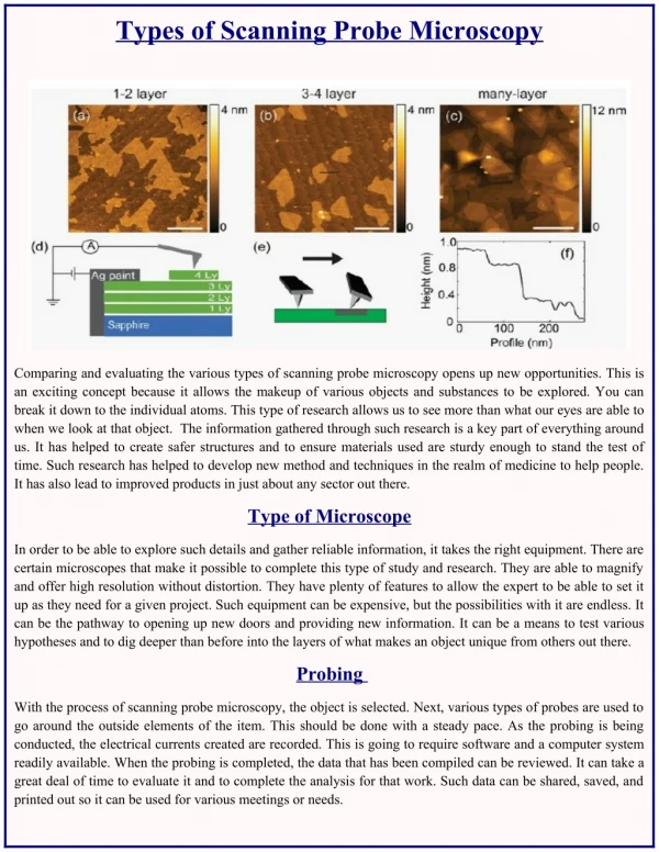
Download
1 / 9
0 likes | 2 Views
Molecular Imaging offers advanced Atomic Force Microscopy (AFM) solutions, enabling researchers to achieve atomic and molecular resolution across various scientific fields. Their modular, customizable systems support applications in biotechnology, materials science, and electrochemistry, providing high-performance imaging with exceptional environmental control. Committed to innovation and precision, Molecular Imaging empowers scientists to explore the nanoscale with unparalleled versatility.<br>

E N D
The Role of Scanning Probe Microscopy in Next-Gen Electronics and Nanofabrication
As the demand for faster, smaller, and more energy-efficient devices continues to rise, the push toward next-generation electronics is more intense than ever. Whether it's quantum computing, flexible electronics, or nanoscale sensors, precision at the atomic level is no longer optional—it's a requirement. And at the heart of this revolution lies a powerful tool: Scanning Probe Microscopy (SPM). From material discovery to nanoscale fabrication, scanning probe microscopy has become a cornerstone technology driving progress in electronics and nanomanufacturing. Brands like Molecular Imaging are leading the way, providing researchers and innovators with the precision tools they need to see, understand, and engineer matter at the atomic scale.
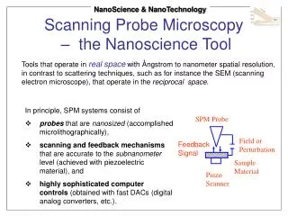
What Is Scanning Probe Microscopy? Scanning probe microscopy refers to a group of techniques that use a physical probe to scan a material’s surface with atomic precision. The most common types—Atomic Force Microscopy (AFM) and Scanning Tunneling Microscopy (STM)—allow scientists to image, measure, and manipulate matter at the nanoscale. Unlike traditional microscopy, SPM doesn’t rely on light or electrons. Instead, it captures surface features by “feeling” them with a nanometer-scale tip. This makes it uniquely suited for characterizing surfaces with extreme accuracy—ideal for modern electronics where the margin for error is virtually zero.
Why SPM Matters in Electronics and Nanofabrication As electronic devices shrink to the nanoscale, traditional fabrication and inspection tools struggle to keep up. This is where scanning probe microscopy shines. 1. Atomic-Level Surface Characterization In semiconductor development, surface uniformity and cleanliness are critical. SPM techniques, especially AFM, provide ultra-high-resolution topography, allowing engineers to detect surface roughness, defects, and contaminants invisible to other techniques.
2. Material Property Mapping Next-gen electronics demand advanced materials—from graphene to 2D semiconductors. SPM not only maps their surfaces but also measures mechanical, electrical, and magnetic properties on a nanoscale. This leads to faster material validation and better device performance. 3. Precision Nanofabrication With SPM, researchers can go beyond imaging. Techniques like dip-pen nanolithography and nanomachining allow precise manipulation of materials, enabling the construction of nano-devices with atomic control. This opens new doors in memory storage, nanoelectronics, and even single-molecule circuits.
4. Failure Analysis and Quality Control As chips and circuits get smaller, identifying failure points gets tougher. SPM helps engineers pinpoint microscopic issues in interconnects, thin films, and transistor gates—making it an essential tool for yield improvement and reliability assurance. Molecular Imaging: Powering the Future with SPM A pioneer in advanced imaging solutions, Molecular Imaging is at the forefront of delivering cutting-edge scanning probe microscopy systems tailored for nanotech applications. Their tools combine the sensitivity of SPM with modern automation, allowing users to go from lab-scale R&D to production-scale diagnostics without skipping a beat. Whether you're a university researcher studying quantum dots or an industrial engineer working on sub-5nm node semiconductors, Molecular Imaging provides the precision and reliability you need.
Real-World Applications Flexible Electronics: Engineers use AFM to evaluate stress and strain on thin films and organic transistors. Quantum Computing: STM enables manipulation of individual atoms, crucial for building qubits. Photovoltaics: SPM is used to study grain boundaries and charge transport in perovskite solar cells.
Medical Devices: Biocompatibility and nanostructure analysis are enhanced with high-resolution SPM scans. Looking Ahead As the world moves toward 6G networks, wearable health tech, and AI-driven hardware, the role of scanning probe microscopy will only become more vital. With tools like those from Molecular Imaging, innovators can explore deeper, fabricate smarter, and push the boundaries of what's possible—one atom at a time. Original Content: https://miafmus.livejournal.com/464.html
Thank You Contact No.:1-888-644-0389 Address: 3485 Middle belt, West Bloomfield, Michigan, 48323 songxu@nanocuetech.com