Download

1 / 2
0 likes | 26 Views
Understanding how semiconductors are manufactured reveals the incredible precision and innovation behind todayu2019s digital world.

E N D
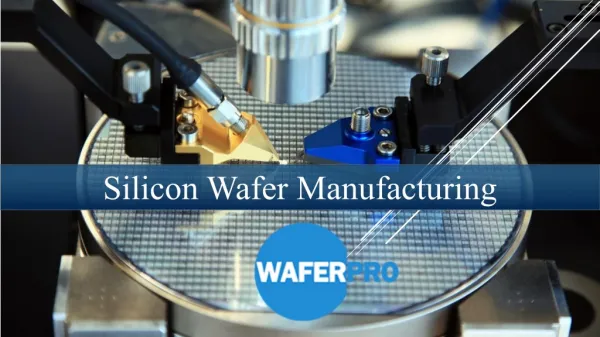
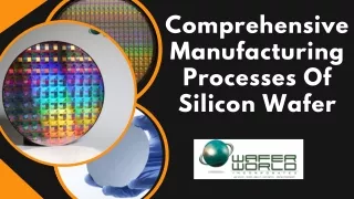
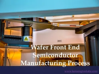
From Sand To Silicon: Understanding The Semiconductor Manufacturing Process Semiconductors are at the core of nearly every modern electronic device, from smartphones to satellites. Their production, however, involves a highly complex and controlled process that transforms raw materials into sophisticated microchips capable of executing billions of calculations per second. Understanding how semiconductors are manufactured reveals the incredible precision and innovation behind today’s digital world. 1. Raw Material Preparation The process begins with silicon, one of the most abundant elements on Earth, typically extracted from sand. Silicon is chosen for its excellent electrical properties and stability. The raw silicon is purified through a chemical process to create polysilicon, which is then melted and grown into a single crystal ingot using the Czochralski method. This cylindrical ingot is sliced into thin wafers, which form the base of semiconductor devices. 2. Wafer Cleaning and Inspection Once sliced, the wafers undergo rigorous cleaning to remove any particles, residues, or defects. These ultra-flat wafers are then inspected using optical tools and measurement systems to ensure they meet strict dimensional and surface criteria. Any variation at this stage could compromise later steps in the process. 3. Photolithography: Patterning the Circuit Photolithography is a key step in defining the tiny structures that form the circuitry of a chip. A photoresist material is applied to the wafer surface, and ultraviolet light is used to transfer a circuit pattern through a photomask. Areas exposed to light are chemically altered, allowing selective removal of the resist. This process is repeated multiple times to create multiple layers of patterns, each corresponding to a part of the final chip architecture. As chip designs become more complex and smaller, photolithography requires highly advanced equipment capable of working at nanometre scales. 4. Etching and Doping After patterning, etching is used to remove material from the wafer surface, forming trenches or holes as defined by the resist. This can be done using wet chemical methods or dry plasma-based processes. Doping follows, which introduces impurities into selected areas of the silicon wafer to alter its electrical conductivity. Ion implantation or diffusion techniques are used to control how electrons move within the device, forming the basis of transistors and other active components. 5. Deposition and Layering Various materials, including metals and insulators, are deposited onto the wafer in extremely thin layers. These layers may form connections between components or serve as insulating barriers.
Techniques like chemical vapor deposition (CVD) or physical vapor deposition (PVD) are used depending on the material and function. 6. Packaging and Testing After all layers are constructed and the wafer is complete, it’s cut into individual chips through a process called dicing. Each chip is then mounted into a protective package that provides electrical connections to the outside world. Before reaching end-users, each chip is rigorously tested for functionality and reliability. Any chip that fails to meet specifications is discarded. Conclusion The semiconductor manufacturing process is a blend of advanced science, engineering, and quality control. With growing demand for faster, smaller, and more efficient devices, this process continues to evolve. Though invisible to most, the technology behind semiconductors is deeply embedded in daily life, powering everything from communication systems to medical equipment and beyond.