Download
1 / 7
90 likes | 281 Views
The Wafer front end production process gets done, the wafers are then transmitted to the assembly facility to save the chip. It assists the integration into the electronic systems, confines the electric interference, and brings the heat from the devices.

E N D
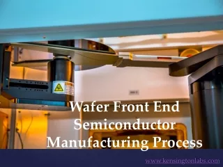
Wafer Front End Semiconductor Manufacturing Process www.kensingtonlabs.com
The emerging manufacturing process on the verge of checking the cleanliness and environmental control is the wafer handling equipment. It has loomed from the semiconductor devices manufacturing within the semiconductor front end industry. The process is carried out for the significant environments where certain factors are checked out, such as temperature, humidity, particle contamination, and controlled with the particular parameters. How the wafers are built up?
If we talk about the semiconductor backend production, it comes in a consignment production form based on many customers' various orders. In this case, the backend companies build the final product with the non-defective dies, which is picked up from the wafer conveyed from the front-end production and makes the products reach their place within the due dates. The information says that only non-defective dies are taken in the final product. Kensington Laboratories fulfill the clients' significant requirements and attempt to provide the comprehensive and best scope of the items from ADOs, end-effectors, and wafer handling robots at a modest rate. Introduction to the front end and back end wafer semiconductor production
Appropriately chemical distribution • No more meters requirements • High quality • Budget-friendly option • Low energy consumption • 360 degrees rotation • Ergonomic design • Easy loading and filling • Customized controls What can we expect from the Wafer Handling Automation?
The Kensington Laboratories presents the 300mm FOUP of secured wafer handling, where the robots are processed with the optical sensing device to analyze the functionality and the environment. It is used to identify whether the wafers are placed at the appropriate place and if in case it is not, where it should be. The Effectiveness of Wafer Handling
AMAT Robots (applied materials robot repair) • Removed from the AMAT applied materials 300mm endure PVD physical vapor deposition system • It consists of non-copper material. Kensington robot stage repair and Newport PM500 stage spare parts field replaceable units are crafted to lessen the downtime and boost productivity. It can be further abruptly and easily installed on-site by the customers without any unique tool or testing. The Newport Wafer Robots Kensington AMAT
Sales – Kensington Robots & Stages, Newport PM500 Stages, Spare Parts sales@kensingtonlabs.com Service - Kensington robot and stage repairs, Newport PM500 stage repairs service@kensingtonlabs.com Kensington Laboratories, LLC 6200 Village Parkway Dublin , CA 94568 Phone: 510.324.0126 Fax: 510.324.0130 www.kensingtonlabs.com CONTACT US Our Toll Free Number 1-888-977-7800