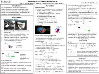
Download
1 / 13
130 likes | 168 Views
In order to design different Systolic Architectures like R1 R2 W1 etc.<br>Follow Design methodology.<br>Construct the Systolic Architecture accordingly

E N D
DESIGN OF R1,R2 and W1 Date:-14/04/2020 Time:-1:00 pm By Huirem Bharat Meitei Ernl No:-19405004 PhD VLSI (ECE) Supervisor Dr.Manoj Kumar Assistant Professor Department of Electronics &Communication NIT Manipur
Contents • Introduction • Systolic Array Design Methodology • DG and Basic Vectors • Design R1 • Design R2 • Design W1 • Alternative Design • Conclusion
Introduction • In order to design different Systolic Architectures like R1,R2,W1,B1,F etc. • Follow Design methodology. • Construct the Systolic Architecture accordingly
Systolic Array Design Methodology Represent the Algorithm as a Dependence Graph Applying Projection, Processor, and Scheduling Vectors(Space-Time Representation) Edge Mapping Construct the Final Systolic Architecture
DG and Basic Vectors • Projection vector dT= [d1d2] • Processor space vector pT= [p1p2] • Schedule vector sT= [s1s2] • Hardware utilization efficiency: HUE = 1/|sTd| Note:- Processor space vector and the projection vector must be orthogonal to each other. P is orthogonal to d, that is, pTd = 0 Basic Vectors
Design R1 Results Stay, Inputs and Weight Move in Opposite Directions STEP 1:- Selection of Projection, Processor, and Scheduling Vectors dT=[1 -1] ,pT=[1 1] ,sT=[1 -1] STEP 2:-Edges Mapping Table:-1 edges mapping of R1 design
STEP 3:- Block diagram Fig 1:- Block diagram of R1 Design STEP 4:- low level implementation Fig 2:- Low level implementation of R1 Design
Design R2Results Stay, Inputs and Weights Move in the Same Direction but at Different Speeds STEP 1:- Selection of Projection, Processor and Scheduling Vectors dT=[1 -1] pT=[1 1] sT=[2 1] STEP 2:-Edges Mapping Table 2:- Edges mapping of R2 Design STEP 3:- Block diagram Fig 3:- Block diagram of R2 Design
Design W1 Weights Stay, Inputs and Results Move in Opposite Directions STEP 1:- Selection of Projection, Processor and Scheduling Vectors dT=[1 0] pT=[0 1] sT=[2 1] STEP 2:-Edges Mapping Table 3:- Edges mapping of W1 Design STEP 3:- Block diagram Fig 4:- Block diagram of W1 Design
ALTERNATIVE DESIGN Table 4:- Other alternative Design
Conclusion • By Proper Determining of projection vector d, processor space vector pT and scheduling vector sT • Designing of systolic Architecture R1,R2 and W1 is achieved from edges mapping.
References • vlsi-digital-signal-processing-keshab-k-parhi • VLSI programming Systolic Designhttp://www.win.tue.nl/~wsinmak/Education/2IMN35/2IMN35-2016-slides-systolic.pdf • Systolic Architecture Design. Lan-DaVan, Ph. D. Department of Computer Science National ChiaoTung University Taiwan,R.O.C.Fall, 2010 4. Why Systolic Architecture? http://www.eecs.harvard.edu/~htk/publication/1982-kung-why-systolic-architecture.pdf
Thanking you Any Quarries ??? “Stay Inside and The Quest For Knowledge Continue….”