Download
1 / 14
231 likes | 811 Views
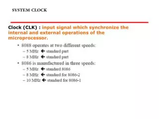
SYSTEM CLOCK. Clock (CLK) : input signal which synchronize the internal and external operations of the microprocessor. CLOCK GENERATOR IC. The clock source is generated by 8284 ( clock generator and Driver IC ) CLK ( 8) of 8284 is connected to pin 19 8088/8086

E N D
SYSTEMCLOCK Clock (CLK) : input signal which synchronize the internal and external operations of the microprocessor.
CLOCKGENERATOR IC • The clock source is generated by 8284 ( clock generator and Driver IC ) • CLK ( 8) of 8284 is connected to pin 19 8088/8086 • 8284 also supplies it with 2 of it's control lines – RESET and READY. The RESET signal does resets the 8088. This line can also be used by other peripherals on the computer so that they reset when the 8088 resets. • READY used to slow down the 8088 ; Dfrom IO circuit thru RD1 and RD2 • A crystal oscillatoris connected between X1 and X2 which provides a FUNDAMENTAL CRYSTAL FREQUENCY. ( FCF) • 33% duty cycle the FCF is divided by 3 internally by 8244 to provide the necessary CLK • output pin pclk provide 50% of duty cycle to drive periperal devices http://en.wikipedia.org/wiki/Crystal_oscillator
BUS CYCLE AND TIME STATES • A bus cycle defines the basic operation that a microprocessor performs to communicate with external devices. • Examples of bus cycle are memory read, memory write, input/output read and input/output write. • A bus cycle corresponds to a sequence of events that starts with an address being output on the system bus followed by a read or write data transfer. • During these operations, a series of control signal are also produced by the MPU to control the direction and timing of the bus. • Each bus cycle consists of at least four clock periods, T1, T2, T3 and T4. • These clock period are also called T-state. • These 4 clock states gives a bus cycle duration of ( 125 ns * 4 ) = 500 ns in a 8-Mhz 8088 • Idle State: no bus activity ; one clock period • Wait state : controlled by READY signal ; inserted between T3 and T4 when READY = 0 . Bus cycle will complete when READY = 1
Bus Cycle and Time States T1- start of bus cycle. Actions include setting control signals to give the required values for ALE, DTR, IO/M putting a valid address onto the address bus. T2 - the RD or WR control signals are issued, DEN is asserted and in the case of a write, data is put onto the data bus. The DEN turns on the data bus buffers to connect the CPU to the external data bus. The READY input to the CPU is sampled at the end of T2 and if READY is low, a wait state TW (one or more) is inserted before T3 begins. T3 - this clock period is provided to allow memory to access the data. If the bus cycle is a read cycle, the data bus is sampled at the end of T3. T4 - all bus signals are deactivated in preparation for the next clock cycle. The 8088 also finishes sampling the data (in a read cycle) in this period. For the write cycle, the trailing edge of the WR signal transfers data to the memory or I/O, which activates and write when WR returns to logic 1 level.
System Timing Diagrams • T-State: • One clock period is referred to as a T-State T-State • An operation takes an integer number of T-States • CPU Bus Cycle: • A bus cycle consists of 4 or more T-States T1 T2 T3 T4
Memory Read Timing Diagrams • Dump address on address bus. • Issue a read ( RD ) and set M/ IO to 1. • Wait for memory access cycle.
Memory Read Timing Diagrams T3 T4 T2 T1 CLK A[15:8] ALE Buffer A[15:0] 8088 A[19:16] A[19:16] S3-S6 AD[7:0] A[15:8] A[15:8] D latch Memory AD[7:0] A[7:0] D[7:0] IO/M D[7:0] Trans -ceiver DT/R DT/R DEN DEN IO/M RD WR RD WR
Memory Write Timing Diagrams • Dump address on address bus. • Dump data on data bus. • Issue a write ( WR ) and set M/ IO to 1.
Memory Write Timing Diagrams T3 T4 T2 T1 CLK A[15:8] ALE Buffer A[15:0] 8088 A[19:16] A[19:16] S3-S6 AD[7:0] A[15:8] A[15:8] D latch Memory AD[7:0] A[7:0] D[7:0] IO/M D[7:0] Trans -ceiver DT/R DT/R DEN DEN IO/M RD WR RD WR
Bus Timing During T 1 : • The address is placed on the Address/Data bus. • Control signals M/ IO , ALE and DT/ R specify memory or I/O, latch the address onto the address bus and set the direction of data transfer on data bus. During T 2 : • 8086 issues the RD or WR signal, DEN , and, for a write, the data. • DEN enables the memory or I/O device to receive the data for writes and the 8086 to receive the data for reads. During T 3 : • This cycle is provided to allow memory to access data. • READY is sampled at the end of T 2 . • If low, T 3 becomes a wait state. • Otherwise, the data bus is sampled at the end of T 3 . During T 4 : • All bus signals are deactivated, in preparation for next bus cycle. • Data is sampled for reads, writes occur for writes.
Setup & Hold Time • Setup time – The time before the rising edge of the clock, while the data must be valid and constant • Hold time – The time after the rising edge of the clock during which the data must remain valid and constant
Bus Timing Timing: • Each BUS CYCLE on the 8086 equals four system clocking periods (T states). • The clock rate is 5MHz , therefore one Bus Cycle is 800ns. • The transfer rate is 1.25MHz. Memory specs (memory access time) must match constraints of system timing. For example, bus timing for a read operation shows almost 600nsare needed to read data. • However, memory must access faster due to setup times, e.g. Address setup and data setup. • This subtracts off about 150ns. • Therefore, memory must access in at least 450nsminus another 30-40nsguard band for buffers and decoders. • 420nsDRAM required for the 8086.
10.6 System Time Diagrams - CPU Bus Cycle T1 T2 T3 TW T4 CLK ALE Address latches store the actual values Memory Cycle (I/O cycle is similar but IO/M = 1) IO/M A16- A19 A16-A19 S3- S6 A8- A15 A8- A15 READY the P samples READY (if 0 a WAIT state follows) The slow device drives READY= 0 Read Cycle (instruction fetch and memory operand read) RD P reads Data Bus AD0- AD7 A0- A7 D0- D7 (Data in) Tri-state DT/R Direction “READ” for the Data Buffer DEN Enables Data Buffer Memory reads Data Bus WR Write Cycle (memory operand write) AD0- AD7 A0- A7 D0- D7 (Data out) DT/R Direction “READ” for the Data Buffer DEN Enables Data Buffer