Download
1 / 2
40 likes | 148 Views
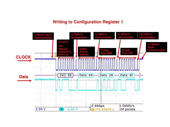
Writing to Configuration Register 1. 8) TMP513 acknowledges. 6) TMP513 acknowledges. 10) TMP513 acknowledges. 4) TMP513 acknowledges. 1) Master Starts Communication. 2) and 3) 7bit address followed by R/W Low. 11) Master Stops Communication. 5) 8bit Pointer Address. 9) Data Byte LSB.

E N D
Writing to Configuration Register 1 8) TMP513 acknowledges 6) TMP513 acknowledges 10) TMP513 acknowledges 4) TMP513 acknowledges 1) Master Starts Communication 2) and 3) 7bit address followed by R/W Low 11) Master Stops Communication 5) 8bit Pointer Address 9) Data Byte LSB 7) Data Byte MSB CLOCK Data
Reading From Configuration Register 1 10) TMP513 acknowledges 4) TMP513 acknowledges 6) TMP513 acknowledges 1) Master Starts Communication 7) Master Starts Communication 12..Cont) Master Acknowledge 11..Cont) Master Acknowledge 2) And 3) 7bit address followed by R/W Low 8) And 9) 7bit address followed by R/W High 5) 8bit Pointer Address 11) Read MSB 12) Read LSB 13) Master Stops Communication CLOCK Data