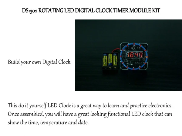
Download
1 / 33
330 likes | 646 Views
CENG3480_B1 Digital System Clock . Reference: Chapter11 of High speed digital design , by Johnson and Graham. Setup time and Time margin. Setup time : The time that the input data must be stable before the clock transition of the system occurs.

E N D
CENG3480_B1 Digital System Clock Reference: Chapter11 of High speed digital design , by Johnson and Graham Clock distributions (v.9a)
Setup time and Time margin • Setup time: The time that the input data must be stable before the clock transition of the system occurs. • Timing margin measures the slack, or excess time, remaining in each clock cycle • Protects your circuit against signal cross-talk, miscalculation of logic delays, and later minor changes in the layout. • Depends on both time delay of logic paths and clock interval. Clock distributions (v.9a)
Example to show the importance of time margin • A 2-bit ring counter • Initially A,B =0 ; A=001100110 • What is B? A B Clock distributions (v.9a) Ans: 011001100
A 2-bit ring counter example (Cont’d) • The result is ok when the clock is slow. • But we may have problems when the clock is too fast. (see next page) Clock distributions (v.9a)
May cause problem if TCLK is too short Clock distributions (v.9a)
A B Exercise B4.1 • Given: • CLK1=CLK2=20MHz, • FF clock-to-Q output delay=8ns; • setup time for FF is 5ns; • Gate delay G is 10ns; • Q1 Q2 are 0 initially. • Questions: • Find time margin. • How many delay G gates can you insert between A and B without creating error? Clock distributions (v.9a)
delay1 delay2 Source clock:CLK0 Clock Skew • The clock does not reach at FF1, FF2 at the same time • E.g. Clock skew =(TC1,max - TC2,min)=1 ns, • a positive skew when TC2,min happens earlier than TC1,max, FCLK0 cannot be too high. CLK0 TCLK1 TC1,max= latest TC1arrival time TCLK2 TC2,min= earliest TC2 arrival time Set t=0 here Skew (T C1,max - T C2,min) A positive skew Clock distributions (v.9a)
Clock source CLK1 CLK2 Clock skew TFF+TG Time t=0 Tc2 Tc1 Tsetup Tclock Skew (T C1,max-T C2, min) FF1 FF2 Clock distributions (v.9a)
Clock skew (at FF1) • Due to the problem when the synchronous clock does not arrive at various components at the same time. • The latest possible arrival time for a pulse coming through gate G is Tslow = TC1,max + TFF,max + TG,max • Tslow=slowest arrival for pulse from G • TC1,max =Max. delay of path C1 • TFF,max =Max. delay, clock to Q of FF1 • TG,max =Max. delay of G, including trace delay Clock distributions (v.9a)
Clock Skew (at FF2, the next cycle) • The arrival time required by FF2 is Trequired = TCLK + TC2,min - Tsetup • Trequired=elapsed time by which data from G must arrive • TCLK=interval between clocks; clock period • TC2,min =Minimum delay of path C2 • Tsetup =worst-case setup time required by FF2, data at D1 must arrive at least Tsetup before CLK2 Clock distributions (v.9a)
Clock Skew (combining delay & setup requirements) • Data from G must arrive before Trequired to properly set FF2. So, • Trequired – Tslow > 0, hence Trequired > Tslow, therefore • TCLK + TC2,min - Tsetup > TC1,max + TFF,max + TG,max • TCLK > TFF,max +TG,max + Tsetup + (TC1,max - TC2,min) + Tsome_margin • Example: assuming • TFF,max = 6ns • Delay between Flip-flops, TG,max + Tsetup = 5ns + 3ns = 8ns • clock skew =(TC1,max-TC2,min)=1ns, a positive skew when TC2,min happens earlier than TC1,max. • Timing margin Tsome_margin = 4ns (make sure the circuit is reliable) • Total = 18ns ==> Fmax= 55.5MHz • Use clock frequency =55MHz would be safe. Clock distributions (v.9a)
Exercise: B4.2 • Given: • TFF,max = 7ns • TG,max= 5ns • Tsetup =4ns • Timing margin Tmargin =3ns • FCLK =40MHz • What is the biggest time skew allowed? Clock distributions (v.9a)
Strategies to reduce clock skew • Two main strategies: • Locate all clock inputs close together; but it is difficult to implement in a large circuit. • Drive them from the same source & balance the delays • Due to physical limitation, strategy 2 is often used • Spider-leg distribution network • use a power driver to drive N outputs. • Use load (R) termination to reduce reflection if the traces are long (distributed circuit). Total load =R/N. • E.g. line impedance=75 , N=3, total load=25. • Two or more driver outputs in parallel may be needed. • Clock distribution tree. Clock distributions (v.9a)
Spider leg Distribution Network Clock distributions (v.9a)
Clock distribution tree Clock distributions (v.9a)
Delay adjustment • The simplest clock adjustment is fixed delay. • Fixed delay: • Delay line by transmission line: short delays 0.1-5ns, 10% variation, accurate. • Gate delays 0.1-20ns, 300% variation, not accurate. • Lumped-circuit delay (RC) • Figure 11.10: 0.1->1000ns, variation 5-20%, accurate. • Adjustable delays • Delay line directly printed on PCB; delay may vary with temperature • Insert a RC circuit between two buffers Clock distributions (v.9a)
Selectable delay adjustment (using jumper) Clock distributions (v.9a)
Selectable delay adjustment (using jumper) • Jumper block will have bigger Capacitance • Use direct solder is better by more difficult to tune Clock distributions (v.9a)
Low Impedance Clock Distribution Line • Three means to reduce reflection pulse heights • Slow the rise & fall time of the driver • Lower the capacitance of each tap • Lower the characteristic impedance of the clock distribution line • Must also try to minimize the parasitic capacitance of the connector and PCB Clock distributions (v.9a)
Differential Distribution • Can survive tougher noise environment • Better signal size (lower amplitude: half) • Differential Balance • ECL signal system is better than TTL Clock distributions (v.9a)
Clock Signal Duty Cycle • Ideal duty cycle: 50% • Falling edge of an ideal clock signal bisects successive rising edge • Average DC value lies halfway between Hi & Lo states • Keeping symmetry is difficult because asymmetry response to rising and falling edge • Different propagation delays TLH & THL • Long chain of identical gates will distort the pulse width, positive pulse may emerge shorter (and vice versa) • Two clever tricks: • Inverts the clock signal at every stage (balance the distortion) • Use analog circuit to reshape the waveform Clock distributions (v.9a)
Analogue circuit to reshape the clock • Tuning is difficult Clock distributions (v.9a)
Cancelling Parasitic Capacitance • When new device is added to a multi-drop line, the parasitic capacitance may cause clock phase shift (a function of the parasitic Capacitance) • Use a negative reactance to cancel the effect • works at a particular frequency only Clock distributions (v.9a)
Clock Generators (Oscillators) • Seldom design our own • Comes in hermetically sealed package • A thick film hybrid circuit on a substrate • More important to understand the requirements Clock distributions (v.9a)
Frequency Specifications • Frequency (Hertz, KHz, MHz, GHz) • Nominal operating frequency or centre frequency • Higher frequency is synthesis by filtering and enhancing harmonics of the crystal’s fundamental operating frequency • Stability • Consolidates variations due to temperature, manufacturing processes, operating voltage and aging • In parts per million (ppm); one-hundred ppm = 0.01 % • Aging • In ppm/year • Younger crystal ages faster • Voltage sensitivity Clock distributions (v.9a)
Allowed Operating Conditions • Temperature • Typically 0 – 70oC • Cause Frequency change • Temperature drift is not linear • Input voltage • Like Vcc spec. for IC • Shock • Refers to mechanical (not electrical) shock • In units of G’s • Apply shock tests in both polarities along all three geometric axes • Vibration • Similar to shock, violently shakes the oscillator • Shock & vibration tests are essential to military or similar products • Humidity • Hermetically sealed package can easily work at any condition Clock distributions (v.9a)
Electrical Parameters • Output type • TTL, CMOS or ECL (10K or 100K) outputs • Maximum loading • Excess load may cause drift • Duty Cycle • More difficult to guarantee at higher frequency • Rise and fall times • Common practice: 10-90% are given in ns • Input current • In milliamps • A function of the Frequency; higher the frequency, more energy is required Clock distributions (v.9a)
Mechanical Configuration • DIP • Half DIP • Surface mount Manufacturing Issues • Solderability • Cleaning • Package leak rate Clock distributions (v.9a)
Reliability • Functional screening (how many did manufacturer test) • Aging at accelerated temperature Bells and Whistles • Differential outputs • Enable • Voltage controlled oscillator (adjust frequency electronically) • Tuning Clock distributions (v.9a)
Other Issues • Clock Jitter • Clock oscillator contains a high frequency amplifier that may resonate • This high frequency signal may appear as noise and appears at the output in the form of clock jitter (superimpose of base signal and higher frequency components) • May cause malfunction • Can use measuring technique and feedback system to control the effect Clock distributions (v.9a)
Need to control Power supply stability • Supply variation will affect the frequency and will appear as noise • Laying clock signal lines also need special attention • Cause lots of noise (cross talk due to high frequency) • Must try to specify, demand special treatment and lay out the clock distribution network first • Use thicker line or isolation grid to make bigger separation from other signals • Use a separate layer Clock distributions (v.9a)
Answer for B4.1 • Clock cycle is (T) 1/20Mhz = 50 ns • Time margin = T- clock_to_Q+ setup_time - delay_G • = 50ns – 8ns-5ns-10ns=27ns • Since each delay is 10ns, so you may add 2 more (totally 3 between A and B). Clock distributions (v.9a)
Answer: B4.2 • TCLK > TFF,max +TG,max+ Tsetup + (TC1,max-TC2,min) +Tmargin • TFF,max = 7ns • TG,max= 5ns; Tsetup =4ns • Timing margin Tmargin =3ns • FCLK =40MHz => TCLK =25ns • Max. Time skew (TC1,max-TC2,min)> TCLK -(TFF,max +TG,max+Tsetup+Tmargin ) =25ns- (7ns+5ns+4ns+3ns)= 6ns. Clock distributions (v.9a)