Download
1 / 23
230 likes | 303 Views
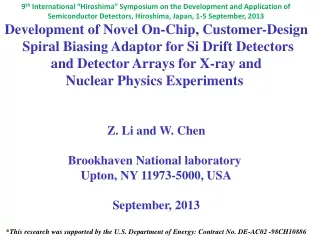
9 th International “Hiroshima” Symposium on the Development and Application of Semiconductor Detectors, Hiroshima, Japan, 1-5 September, 2013. Development of Novel On-Chip, Customer-Design Spiral Biasing Adaptor for Si Drift Detectors and Detector Arrays for X-ray and

E N D
9th International “Hiroshima” Symposium on the Development and Application of Semiconductor Detectors, Hiroshima, Japan, 1-5 September, 2013 Development of Novel On-Chip, Customer-Design Spiral Biasing Adaptor for Si Drift Detectors and Detector Arrays for X-ray and Nuclear Physics Experiments Z. Li and W. Chen Brookhaven National laboratory Upton, NY 11973-5000, USA September, 2013 *This research was supported by the U.S. Department of Energy: Contract No. DE-AC02 -98CH10886
Outline Introduction Concept of Spiral Biasing Adapter (SBA) --- Separation of biasing and SDD field-define-rings Design of SBA Design of SDD cell Some design options of SBA and SDD First protypes Summary
1 Introduction The current Spiral SDD was designed such that each SDD single cell has its own biasing spiral, which is also used as the definition of the p-n junction on the surface [1-3]; The power is therefore Ps=Vout2/Rspiral (1002/10M=1 mW/cell) for a single cell and P=N2xPs for a SDD array of NxN, which can be large (e.g. for N=100, P=10 W) ; The heat generated by this power stays with the SDD, making it hard to cool down necessary for low leakage current;
Introduction (continue) The new SBA a) will separate the biasing and p-n junction definition b) is designed and processed the same as SDD in geometry and in wafer; c) less powers consumption (one SBA per SDD array); d) SDD has the same geometry as SBC (i.e. pitch p=p(r) ); implant width W=W(r) can be 80 to 90% of p(r) --- minimum surface area; Only a few bonds are needed to connect SBA and SDD; It may stay on the same SDD chip (not severed off) for easy one metal/two metal connections to the SDD The biasing on the SDD array can be interconnected by one or two metal process depending on the value of Vout;
Spiral square SDD single Cell ---- Good for packing in space Spiral implants used to define a constant drift field --- minimum drift time Vout VBout n+ anode Vanode=0 Vout VE1 VBE1 e VE1 I p+ spirals e Vanode=0 IB e e e VBout VBE1 If we only bias VBE1 (or bias VBE1 = VBout, =0), it will be the same as biasing the backside uniformly
Square SBA Chip A 1500 m V
Square SBA Voltage distribution on SBA bias voltage Linear dependences
Square SBA Chip 1500 m Al wire bonds Square SDD Array
Design of SBA Chip integrated with SDD and SDD arrays Detector processing will soon begin
Square SBA Chips Square SDD Array
Square SBA Chips Square SDD Array
Square SBA Chips Square SDD Array
Square SBA Chips Square SDD Array
7 Summary Novel On-Chip Spiral Biasing Adapter (SBA) has been proposed SBA has achieved the separation of biasing and SDD field-define-rings Design of SBA and SDD rings are competiple First prototype of SBA has been made First protype of SBA with SDD is on the way References [1] P. Rehak et al., “Spiral Si Drift Detectors”, IEEE Trans. Nucl. Sci., Vol. 36, No. 1, 203-209 (1989) [2] P. Rehak et al.,”Array of Silicon Drift Detectors for an Extraterrestrial X-ray Spectrometer”, Nucl. Instr. and Meth. A, 624, 260-264 (2010) [3] W. Zhang et al., IEEE Trans. Nucl. Sci., Vol. 47, No. 4, 1381-1385 (2000) [4] Z. Li, , Nuclear Instruments & Methods in Physics Research A (2013), http://dx.doi.org/10.1016/j.nima.2013.06.066i