Download
1 / 26
330 likes | 541 Views
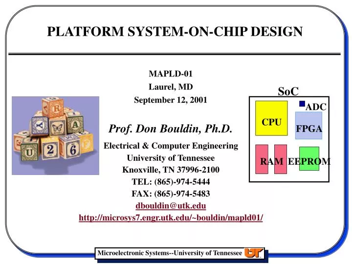
SoC. ADC. CPU. FPGA. RAM. EEPROM. PLATFORM SYSTEM-ON-CHIP DESIGN. MAPLD-01 Laurel, MD September 12, 2001 Prof. Don Bouldin, Ph.D. Electrical & Computer Engineering University of Tennessee Knoxville, TN 37996-2100 TEL: (865)-974-5444 FAX: (865)-974-5483 dbouldin@utk.edu

E N D
SoC ADC CPU FPGA RAM EEPROM PLATFORM SYSTEM-ON-CHIP DESIGN MAPLD-01 Laurel, MD September 12, 2001 Prof. Don Bouldin, Ph.D. Electrical & Computer Engineering University of Tennessee Knoxville, TN 37996-2100 TEL: (865)-974-5444 FAX: (865)-974-5483 dbouldin@utk.edu http://microsys7.engr.utk.edu/~bouldin/mapld01/
Silicon Manufacturing Design Productivity Crisis System on Chip Designs Impact of Design With Reuse Requirements for Reuse Acquiring Reusable Components Design With Reuse Strategies Prototyping Choices ARM OUTLINE OF THIS PRESENTATION http://www.eecs.umich.edu/~brown/
IC Shrinks CPU Base Design SoC ADC CPU FPGA Or Keep Package Same Size RAM EEPROM MOORE’S LAW:2X FUNCTIONALITY EVERY 18 MONTHS CPU
DESIGN PRODUCTIVITY LAGS MANUFACTURING CAPABILITY Maya Rubeiz USAF Wright Labs maya.rubeiz@sn.wpafb.af.mil http://rassp.scra.org
A SYSTEM-ON-CHIP CAN REUSE COMPONENTS • EACH COMPONENT MUST • BE “KNOWN GOOD” • DETAILED INFORMATION • IS REQUIRED • FOR SUCCESS • BEST WHEN COMPONENTS • ARE DESIGNED FOR • REUSE http://microsys6.engr.utk.edu/ece/research/microsys/dsp_mcm/
0.9 1.0 0.9 1.0 0.9 0.9 0.9 0.9 0.9 1.0 1.0 1.0 Interconnect 0.9 Interconnect 0.9 UNPROVEN COMPONENTS AND INTERCONNECT ARE RISKIER AND MORE TIME-CONSUMING TO VERIFY 0.9x0.9x0.9x0.9x0.9x0.9x0.9 = 0.5 1.0x1.0x1.0x1.0x1.0x0.9x0.9 = 0.8
WE BUILD SKYSCRAPERS USING STANDARDIZED BLOCKS So, let’s use standardized blocks to build systems
Design #1 without Planned Reuse Design #2 without Planned Reuse Design #3 without Planned Reuse 1.5 1.8 2.1 Design #2 WITH IP Design #3 WITH IP Design # 1 For Reuse IP blocks should have well-defined interfaces Often, IP are more like patches that must be stitched together like a quilt DESIGN WITH REUSE CAN HAVE A SIGNIFICANT IMPACT
BASICS: HDL Models Functional Description Application Intent Interface Specifications Authors and Owners Size, Delay, Power Estimates Packaging Info REQUIREMENTS FOR REUSABLE IP • ALSO NEED: • Test Bench (Input Stimuli/Output Responses • Tools and Versions Used/Needed • Foundry Used For Fab • Size, Delay, Power Measurements • Testability Features (BIST, JTAG, SCAN)
IP Design Center IP Foundry ASIC/FPGA LOW-RISK IP CAN ATTRACT BUSINESS BUT PRICES MAY NOT BE COMPETITIVE CUSTOMER
REPOSITORY www.design-reuse.com Foundry Foundry Foundry AN OPEN COMPETITIVE MARKET HAS BEEN INITIATED CUSTOMER PORTABLE IP (Multiple Suppliers) Standards: www.vsi.org ASIC/FPGA
STAR IP: Blocks requiring 100+ staff years to design (like ARM, MIPS ) have become bestsellers and come with lots of support. Small IP: Blocks requiring 1-2 staff years to design are priced at 1/3 of the development cost. Buyers are skeptical about the value and often prefer to do these in-house. Medium IP: Blocks requiring 5-10 staff years are profitable for both seller and buyer. However, some suppliers have been bought by foundries to add to the foundries’ captive portfolios. MARKETPLACE EXPERIENCES
LEON is an open-source 32-bit SPARC V8 CPU that was developed by the European Space Agency and is available for free at www.leoncenter.com An open-source 8051 CPU is available for free at www.cs.ucr.edu/~dalton/i8051/ An open-source 68HC11 CPU is available for free at www.gmvhdl.com/hc11core.html OPEN-SOURCE CPUS FOR FREE
www.st.com/stonline/prodpres/dedicate/auto/embedded/st10.htm REDUCING RISK OF DESIGN WITH REUSE • To reduce the risk of reusing multiple, unproven components, an organization may design a SoC platform. • Then, derivative designs with a few new components can be designed rapidly.
HW-SW Kernel + Reference Design Pre-Qualified/Verified Foundation-IP* Scaleable bus, test, power, IO, clock, timing architectures MEM Application Space Hardware IP Processor(s), RTOS(es) and SW architecture CPU FPGA SW IP Reconfigurable Hardware Region (FPGA, LPGA, …) Programmable *IP can be hardware (digital or analogue) or software. IP can be hard, soft or ‘firm’ (HW), source or object (SW) Foundry-Specific HW Qualification SW architecture characterisation SOC PLATFORM DESIGN gmartin@cadence.com
FPGAs can contain soft or hard IP (including CPUs). www.atmel.com www.altera.com www.triscend.com www.xilinx.com RECONFIGURABLE FPGA-BASED BOARDS CAN PROTOTYPE DIGITAL DESIGNS
APPLICATION REQUIREMENTS TEAM PROJECT HDL HDL HDL HDL DESIGN FOR REUSE FPGA FPGA FPGA FPGA VERIFICATION DESIGN WITH REUSE SYSTEM INTEGRATION SoC DESIGN-FOR-REUSE and DESIGN-WITH-REUSE
High performance ASICs can now contain programmable logic (embedded FPGA tiles) as needed for flexibility. ARM SOC WITH RECONFIGURABLE COMPONENTS www.lsil.com www.adaptivesilicon.com
A matrix of configurable analog opamps and interconnect can be used to perform filtering and other signal conditioning operations. CONFIGURABLE ANALOG ARRAYS www.anadigm.com www.latticesemi.com
Conventional Transistor Layout Radiation-Tolerant Layout S G D S D G Radiation Effects REF: cern.ch Current (Drain) Desired Behavior Voltage (Gate) RADIATION-TOLERANT CIRCUITS CAN BE MADE USING CONVENTIONAL PROCESSES
SHARING MULTI-PROJECT MASKS AND WAFERS SAVES MONEY Single-User Wafer Shared, Multi-Project Wafer www.mosis.org
MULTI-PROJECT SERVICES PROVIDE ACCESS TO STATE-OF-THE-ART COMMERCIAL PROCESSES
TSMC 0.35µ TSMC 0.25µ 5-metal, 2-poly TSMC 0.18µ 6-metal 2.5/3.3v I/O, 1.5/1./8v Core Peregrine SOI-SOS 0.50µ TSMC 0.15µ TSMC 0.13µ 6-metal, 1 poly, silicided, Cu IBM SiGe 0.5µ IBM SiGe 0.25µ PROCESSES AVAILABLE VIA MOSIS NOW NEXT 6 MONTHS www.mosis.org
Assemble individual components using a board with reconfigurable interconnect to finalize the system specs. Model the entire system and simulate at a high level. • Design and prototype an analog I.C. via MOSIS or CMP. • Design and prototype the digital components using FPGAs. SoC • Integrate the analog and digital sections into a single SoC. STEPS IN MIXED-SIGNAL SOC DEVELOPMENT
We must reuse previous designs to exploit IC manufacturing. Designs must be well-documented and well-understood. Design-for-reuse and design-with-reuse take time and effort. Verification can be done using simulation and prototyping. Proven components can be verified in less time. Platform design can reduce risk and attract business. Digital and analog designs can be prototyped using reconfigurable systems. FPGA chips can contain soft or hard CPU cores. Radiation-tolerant designs can be made using conventional processes. Multi-project brokers provide inexpensive state-of-the-art fabrication. SUMMARY