Download
1 / 18
190 likes | 332 Views
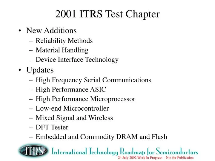
2001 ITRS Test Chapter. New Additions Reliability Methods Material Handling Device Interface Technology Updates High Frequency Serial Communications High Performance ASIC High Performance Microprocessor Low-end Microcontroller Mixed Signal and Wireless DFT Tester

E N D
2001 ITRS Test Chapter • New Additions • Reliability Methods • Material Handling • Device Interface Technology • Updates • High Frequency Serial Communications • High Performance ASIC • High Performance Microprocessor • Low-end Microcontroller • Mixed Signal and Wireless • DFT Tester • Embedded and Commodity DRAM and Flash
2001 Key Challenges • High Speed Device Interfaces • Highly Integrated Designs & SOCs • Reliability Screens • Manufacturing Test Cost Reduction • Test Software Standards • Modeling and Simulation
Demand for Bandwidth • Penetration of high speed interfaces into new designs is increasing dramatically • Learning rate for ATE solutions lags leading edge device technology • Test and DFT methods must be developed to enable development and production test of these products
High Integration Devices & SOC • Customer requirements for form factor and power consumption are driving a significant increase in design integration levels • Test complexity will increase dramatically with the combination of different classes of circuits on single die or within a single package • Disciplined, structured DFT is a requirement to reduce test complexity • New test methods and equipment architectures must be developed • Enable a merge of logic and analog test capability with the throughput of high density memory test equipment
Reliability Screens Run Out of Gas • Critical need for development of new techniques for acceleration of latent defects • Burn-in methods limited by thermal runaway • Lowered use voltages limits voltage stress opportunity • Difficulty of determining Iddq signal versus “normal” leakage current noise • New materials • Rate of introduction increasing: Cu, low k, high k, SiGe • Increasing mechanical sensitivities • Rapid growth of Fabless business model • Organizational and corporate boundaries - lack of clear ownership of reliability in distributed business models
Scaling Component Test Cost • Recent steps have enabled test cost to begin to scale across technology nodes • Equipment reuse across nodes • Increasing test throughput • Challenge remains in most segments, especially high speed and high integration products
Dismantling the Red Brick Walls • Design For Test enabling has begun to remove many of the roadblocks that appeared in the 1997 and 1999 roadmaps • Test is becoming integrated with the design process • Improvements demonstrated in capability and cost • Continued research is needed into new and existing digital logic fault models toward identification of true process defects • Development of Analog DFT methods must advance • Formalization of analog techniques and development of fault models
Test Software Standards Focus • Standards for test equipment interface & communication are needed to decrease equipment factory integration time • Improve equipment interoperability to reduce factory systems integration time • e.g, built into 300mm equipment specifications • Standards for ATE software and test program generation are needed to decrease test development effort and improve time to market • Lower the barrier for selecting the optimal equipment • Increased focus for standards development and adoption of existing standards
How can we improve manageability of the divergence between validation and manufacturing equipment? Can ATE instruments catch up and keep up with high speed serial performance trends? Can DFT mitigate analog test cost as does in the digital domain? What is the cost and capability optimal SOC test approach? What happens when high speed serial interfaces become buses? How can we make test of complex SOC designs more cost effective? Will market dynamics justify development of next generation functional test capabilities? Can DFT and BIST mitigate the mixed signal tester capability treadmill? What other opportunities exist? Will increasing test data volume lead to increased focus on Logic BIST architectures? What are the other solutions?
BISR/BIRA Path Delay Test Strategy Analog Isolation BOST Scan+ATPG IP Core Isolation BIST Analog DSP Control Memory Logic MCU IP Core Based Design Test Implications of IP Design • Test Strategy and Integration • DFT for IP Core Based Design • Higher Level DFT • Standardization
IP Core Test Wrapper Insertion SoC Test Wrapper DFT DFT Test Data Test Data Conversion Test Controller Chip-Level Test Data Configuration of Chip-Level Test Controller and Test Access Mechanism Automated DFT Insertion • Automation of test control integration and test scheduling • Insert test wrapper and test control circuits
Preliminary Roadmap for Handlers Memory 2001 2002 2003 2004 2005 2006 2007 2010 2013 2016 Note Parallel Testing per head 32 to 64 64 to 128 Index Time Sec. 3 to 5 2 to 5 2 to 4 Throughput thousands / hour 6 to 8 8 to 10 8 to 12 Temp. Control degree -55 to 100 Temp. Accuracy degree +/- 3 +/- 2 +/- 2 +/- 1.5 *1 Foot Print ratio 1 to 1.3 1.3 to 1.5 *2 Logic 2001 2002 2003 2004 2005 2006 2007 2010 2013 2016 Note Parallel Testing per head 4 8 16 Index Time Sec. 0.3 to 0.4 to 0.25 Throughput thousands / hour 4 to 6 8 to 12 9 to14 12 to 20 Temp. Control degree Room Temp. to 125 Temp. Accuracy degree +/- 3 +/- 2 +/- 2 +/- 1 *1 Foot Print ratio 1 1.2 1.4 *2 *1 Though 128 become number of parallel testing after 2005 years, it is difficult to keep the temperature accuracy that 64 are the same as the number of parallel testing with memory handler.Therefore, it becomes yellow. Though 8 become number of parallel testing after 2004 years, it is difficult to keep the temperature accuracy that 4 are the same as the number of parallel testing with logic handler. Therefore, it becomes yellow. *2 It is expressed by the index number when 32 of parallel testing in 2001 is made 1. (Therefore, it becomes 1.3 by 64 of parallel testing in 2001.).
Device flow Tray flow Temp. control Parallel testing Achieving the same temperature accuracy in handlers with 128 devices handled in parallel, as handlers with 64 will be very difficult and challenging. Memory 64 to 128 (2005) Logic 4 to 8 (2004) to 16 (2010) Index time Make the handling faster. Make the conveyance distance shorter. More accurate positioning will make the handling time shorter. Device Handler is required to handle diversifying various kinds of packages. Socket Tray Test frequency JEDEC Keep an electrical stable contact Loader UnLoader Foot print Test head Considering the size of the handler needed to access the test floor, the test floor layout, and other transportation restrictions, the handler width should not exceed 1.8 m. The test head size is becoming larger year by year. Preliminary Roadmap for Handlers
Preliminary Roadmap for Sockets Electrical stable contact is one of key technologies on semiconductor device testing. Important contact technologies: Probing contact for wafer testing Discussed in 2001 Socket contact for package testing Proposal for 2002 discussion
Preliminary Roadmap for Sockets Molded board type 2001 2002 2003 2004 2005 2006 2007 2010 2013 2016 Inductance nH 3 to 8 2 to 8 Contact stroke mm 0.3 to 0.5 Contact pressure g 20 to 40 20 to 40 Contact resistance mOhm 30 Guarantee marginal value durability 10000 Note The performance has ripened and there is no big change. Contact pressure is difficult at lead free correspondence. Spring probe type 2001 2002 2003 2004 2005 2006 2007 2010 2013 2016 Inductance nH 2 to 8 1 to 8 Contact stroke mm 0.3 to 0.5 0.3 Contact pressure g 20 to 40 13 to 40 13 to 28 Contact resistance mOhm 150 100 Guarantee marginal value durability 10000 10000 10000 Note The limit over the diameter reduction of a terminal is in sight. New generation type 2001 2002 2003 2004 2005 2006 2007 2010 2013 2016 Inductance nH 1 to 8 Contact stroke mm 0.1 to 0.3 Contact pressure g 13 to 28 Contact resistance mOhm 30 Guarantee marginal value durability 10000 Note If opposite cost is taken into consideration, at a present stage, it is not practical. * Guarantee marginal value : The number of times of a use limit which an offer company guarantees.
Preliminary Roadmap for Sockets A trend of Socket Need to develop novel contactor such as zero-force architecture for ultra high pin counts (narrow pitch) and high speed device testing. Surface mount type of stamping Surface mount of stamping contact pin with rubber component Peripheral Leaf spring type Particle inter-connect ? Spring probe system Barrel less type of spring probe pin One side actuating type of spring probe pin Leaf spring type Area Array Film type Rubber type Micro-spring ?
Modeling and Simulation Difficulty of test development for design & Virtual tester tech. De fac’to program description Test Board verification tech. Correct test Correct test program? equipment? ・Tester resource problems (timing,pattern length, etc.) ・wrong wiring ・ miss relay control point ・ Ground noise ・wrong parts ・probe card (inductance) ・reflection(missmatched Z) ・Tester limitation(clump) ・Wait time ・Different tester Difficult triangular ・ ・ ・ ・ ・ ・ ・ ・ ・ ・ Correct products? ・imperfect circuit understanding ・not fix test spec. ・complex conditions of timing etc ・・・・ Virtual test operation Virtual tester technology
Modeling and Simulation Test board Socket / Probe Machine figure presentation, target electrical property presentation Equivalent length wiring, target transmission impedance Socket/ Probe Small board Socket Test board A large number are taken. Block ring Formation of many pins Workability, Speed Test - Board Conversion board Formation of a special package Conversion Optimize wiring , Adjust processing Electric circuit parameter extraction Tester pin electronics Tester Tester mother board (Electro magnetic analysis) (Board analysis) DR x CP Test board verification technology DUT- Tester transmission New business 1V 3V The necessity for a model 25Ω R L ∽ R 24mA -24mA S CP 350mH CP output SPICE and IBS model Distributed Model, Tester Mode tr=2.0ns/tf=2.4ns tr=1.3ns/tf=1.8ns 6 V tr=2.3ns/tf=12.8ns (Tester transmission way analysis technology) (Customer board design consideration) Device improvement in the speed, customer situation consideration It is overly high-speed testing. High frequency Transition line consideration (RAMBUS, cellular phone) L/R Circuit DiodeClampCircuit I-LOADCircuit Fig 2T6672 Tester Ringing Countermeasure Method Output voltage, current regulation Concentration constant (Voh,Vol,Ioh,Iol (Comparator capacity, driver impedance) Device Tester High-speed tester (125MHz) test mode waveform analysis Subject: socket / probe, a test board, and a tester Even if each shows information, the whole test board verification is difficult.