Download
1 / 7
70 likes | 160 Views
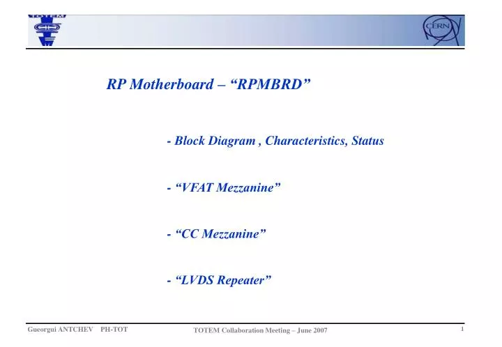
RP Motherboard – “RPMBRD” - Block Diagram , Characteristics, Status - “VFAT Mezzanine” - “CC Mezzanine” - “LVDS Repeater”. VFAT 1. VFAT 1. VFAT 1. VFAT 1. Data Out, S. Detector. Detector. Detector. Detector. VFAT 2. VFAT 2. VFAT 2. VFAT 2. LV,HV. For DOHM.

E N D
RP Motherboard – “RPMBRD” - Block Diagram , Characteristics, Status - “VFAT Mezzanine” - “CC Mezzanine” - “LVDS Repeater”
VFAT 1 VFAT 1 VFAT 1 VFAT 1 Data Out, S Detector Detector Detector Detector VFAT 2 VFAT 2 VFAT 2 VFAT 2 LV,HV For DOHM Trigger PT100 For DOHM T1, MCLK, I2C, Scan VFAT 3 VFAT 3 VFAT 3 VFAT 3 GOH 1 LVDS to CMOS VFAT 4 VFAT 4 VFAT 4 VFAT 4 GOH 2 LVDS to CMOS 40 LVDS Data Out LVDS to CMOS GOH 3 QPLL PLL25 Buffers T1,MCLK LVDS to CMOS GOH 4 RP Hybrids 1 … 10 S (1,3,5,7,9) TR VFAT CC ODD TR Data Out REPEATERS S (2,4,6,8,10) CC EVEN GOH 5 LVDS to CMOS Data Out, S RAD MON I2C CCUM T1, MCLK, I2C, Scan RP Motherboard – “RPMBRD” (1) Block Diagram
LVDS Trigger GOH 4 LVDS to CMOS LVDS with Repeaters - 32 Outputs Coincidence Chips: - 10 x 16 Trigger Outputs TR Data Out TR VFAT S (1,3,5,7,9) CC ODD REPEATERS REPEATERS S (2,4,6,8,10) CC EVEN TR Data Valid LVDS to CMOS GOH 5 Trigger VFAT: - receive 32 Trigger Outputs from LVDS to CMOS converters; - receive T1 from PLL25; - send TR Data Out to the Data Stream (via GOH3); - send TR Data Valid to GOH4 and GOH5; Optical via - GOH4 and GOH5 - Data Valid from: TR VFAT or CCU or TR VFAT S1 bit RP Motherboard – “RPMBRD” (2) Zoom on Trigger outputs
RP Motherboard – “RPMBRD” (3) Cassette + Front Panel + Layout • Pending final verification before production of few prototypes;
VFAT and CC mezzanines • VFAT Mezzanine: • Also Trigger VFAT (for RP Motherboard); • One chip with 32 inputs; • Standard 50pins output connector • Several PCB produced, 1 mounted and under test • CC Mezzanine: • One Coincidence Chip (CC) – on Hungary responsibilities; • 80 LVDS inputs; • 16 LVDS outputs; • I2C control • Design review – done, remarks sent to designer, waiting for • answer
LVDS Repeater • LVDS Repeater: • Repeat 16 LVDS signal lines; • Chip in package; • D-SUB 37pins male/female connectors; • Placed inside plastic hood; • Schematic – done • Chip package definition and layout - pending
Conclusions RP Motherboard – “RPMBRD”: - Design is finish, Final verification; - Production, Order of Components and Tests – pending; - “VFAT Mezzanine” – prototype produced, to be tested; - “CC Mezzanine” – waiting for answer, no price, no delivery date yet ... - “LVDS Repeater” – package definition and layout pending