Download
1 / 21
230 likes | 498 Views
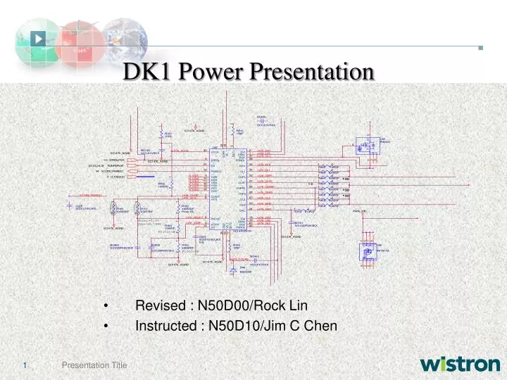
DK1 Power Presentation. Revised : N50D00/Rock Lin Instructed : N50D10/Jim C Chen. DK1 Block Diagram. Power on sequence block diagram. Please link to >>>>>>. Procedure Of Checking KBC Pulses. 1) Use probe to touch the CN11 pin 2 ( DEBUG_TXD ) without inserting AC adapter.

E N D
DK1 Power Presentation • Revised: N50D00/Rock Lin • Instructed: N50D10/Jim C Chen
Power on sequence block diagram • Please link to >>>>>>
Procedure Of Checking KBC Pulses 1) Use probe to touch the CN11 pin 2 ( DEBUG_TXD ) without inserting AC adapter. 2) As for oscilloscope, set up Trigger Mode : Normal. 3) Final step that have to insert AC adapter but do not press Power Button. 4) Eventually, we should have 4 set of pulses as below.
Good Sign From KBC volt/div: 1.00V time/div: 100us
Procedure Of Checking KBC Pulses a) If we couldn't have such pulses fromKBC. b) Please go back to check the signal step by step. ACAV_IN MAX1999_SHDN# 3D3V_S5 X1( PIN 1, 2, XTAL ) DEBUG_OUT. c) There are several circuit portion listed below.
Procedure Of Checking KBC Pulses 32KHz clock for KBC
Procedure Of Checking KBC Pulses DEBUG_TXD from KBC
Procedure Of Checking No Power Issues • Symptom : 3 LED light turn on entirely (FPC) First Case: a) Firstly, you can jump to check VCC_CORE_S0 power plane. b) Does CPU power comes up? c) If doesn't . Please go back to check with the power sequence from beginning as 5V_S3/+3VSRC SUSPWROK 1D8V_S3/1D5V_S3 RUN_ON_D 1D05V_S0 VCC_CORE_S0 . d) These action will check which power plane have no power up. e) The more detailed power sequence waveform have attached from page 12 to page 21.
Procedure Of Checking No Power Issues Second Case: a) Assumed that CPU voltage can attain 0.9 Volt above. b) We may prove that the rest of power plane before VCC_CORE_S0 power plane would be fine. c) Afterward, please check with ICH_PCIRST# H_CPURST# . ( See fig.1, fig.2 below ) d) If ICH_PCIRST# still can’t exist, we can check the following signal : RESET_OUT#( From KBC) VRM_PWRGD. e) If H_CPURST# can’t driven high, the following action should take is checking the GMCH_PWROK( R431 pin 2 ). f) In addition, we can check whether reference voltage (2/3 VCCP) for GMCH correct or not, that is, GTLREF, H_VREF. ( R38 pin 1, GTLREF ), ( R311 pin 1, H_VREF ).
Fig.1 ( H_PWRGD, ICH_PCIRST# ) CH 1 CH 3
Procedure Of Checking No Power Issues 1) If both H_PWRGD and H_CPURST# driven high as fig.1, fig.2. We’ll keep tracking the next signal which connect between CPU and GMCH, that is, H_ADS#. ( Fig.3 ). 2) We can assume that CPU may failure if we can’t get these pulses in Fig.3. 3) Another case is only show up one pulse in Fig.3 that we can suspect the failure in U40 ( Bios Rom ).
Fig.3 ( H_ADS# ) H_ADS# is the “first signal” generated by CPU ,
LPC_LFRAME# WAVEFORM COME OUT AFTER H_ADS# PRODUCED BY CPU ( REFER TO PAGE 20 ) LPC_LFRAME#
By the way, If above signal OK. Then we can check the rest of CLK waveforms.1) Check U62 ( clock GEN ) RN45, RN46 pin 3, 4 CPU CLK ( 100/133 MHz ).
2) Check memory CLK ( 200/266 MHz ) which asserts from GMCH. Practically, we can probe the DDR socket ( normal type ) at pin 35, 37.
CPU access BIOS data flow VCC Clock VCC Clock VCC Clock VCC Clock CPU H_ADS# N/B DMI_RXP/N S/B LPC_LFRAME# BIOS H_TRDY# DMI_TXP/N LPC_LAD(3:0) Reset Reset H_CPURST# H_D#(63:0)
Test Purpose: To record the timing sequence for the power rails. Overview of Procedure: Measure the timing of the power rails. The definition of these timing variables is given in the power sequencing document attached below this table. Timing Variable Time Comments T01 60.00 us Time of AD+ to DCBATOUT T02 200.00 us Time of AD+ to ACAV_IN T03 20.00 us Time of DCBATOUT to +3D3VRTC T04 31.20 us Time of ACAV_IN toMAX1999_SHDN# T05 2.18 ms Time of MAX1999_SHDN# to 3D3V_S5 T06 176.00 us Time of MAX1999_SHDN# to 5V_S5 T06-1 32.7ms Time of 3D3V_S5 to EC_RST# T07 59.20 ms Time of SYS_PWRB# to +3V_SRC T08 329.00 ms Time of SYS_PWRB# to AUX_EN# T09 61.20 ms Time of SYS_PWRB# to SUS_ON T10 380.00 us Time of SUS_ON to 5V_S3 T11 400.00 us Time of SUS_ON to 3VSUS_ON T12 268.00 ms Time of SUS_ON to +15V T13 2.58 ms Time of SUS_ON to ICH_RSMRST# T14 1.40 ms Time of 3VSUS_ON to 3D3V_S3 T15 16.00 us Time of 5V_S3 to +15V T16 1.51 ms Time of 5V_S3 to SUSPWROK_1999 T17 2.21 ms Time of 5V_S3 to ICH_RSMRST# T18 820.00 us Time of SUSPWROK_1999 to 1D5V_S3 T19 2.98 ms Time of SUSPWROK_1999 to 1D8V_S3 T20 1.94 ms Time of 1D8V_S3 to DDR_VREF_S3 T21 98.00 ms Time of ICH_RSMRST# to ICH_SLP_S3# T22 98.40 ms Time of ICH_RSMRST# to RUN_ON T23 106.00 ms Time of ICH_RSMRST# to RUN_PWROK T24 1.08 us Time of ICH_SLP_S3# to PM_PWRBTN# T25 752.00 us Time of ICH_SLP_S3# to 5V_S0 T26 248.00 us Time of ICH_SLP_S3# to 1D5V_S0 T27 2.02 ms Time of ICH_SLP_S3# to RUN_ON_D T28 400 us Time of RUN_ON_D to 3D3V_S0 T29 576.00 us Time of RUN_ON_D to 2D5V_S0 T30 1.21 ms Time of RUN_ON_D to 1D05V_S0 T31 6.52 ms Time of RUN_ON_D to RUN_PWROK T32 6.14 ms Time of 3D3V_S0 to RUN_PWROK T33 1.78 ms Time of RUN_PWROK to VCC_CORE_S0 T34 140.00 us Time of VCC_CORE_S0 to CLK_PWRGD# T35 Time of VCC_CORE_S0 to VRM_PWRGD 4.54 ms T36 -7.60 ms Time of VCC_CORE_S0 to RESET_OUT# T37 4.42 ms Time of CLK_PWRGD# to VRM_PWRGD T38 145.00 ms Time of RESET_OUT# to ICH6_PWROK T39 1.04 ms Time of ICH6_PWROK to ICH_PCIRST# T40 992.00 us Time of ICH_PCIRST# to H_CPURST# Section Owner: Jim C Chen Section Tester: Abel Chang Time To Complete: 06/15 Date Finished: 06/15 DK1 POWER SEQUENCE WAVEFORM