Download
1 / 30
300 likes | 309 Views
Serial Peripheral Interface Bus SPI. SPI Bus. Developed by Motorola in the mid 1980’s. Full-duplex, master-slave serial bus suited to data streaming applications for embedded systems. Existing peripheral busses (UART, I2C) offered inadequate bandwidth and required overly complex control.

E N D
SPI Bus Developed by Motorola in the mid 1980’s Full-duplex, master-slave serial bus suited to data streaming applications for embedded systems Existing peripheral busses (UART, I2C) offered inadequate bandwidth and required overly complex control Objectives included low overhead (point-to-point, no “packets” or complex data framing, synchronous, no complex processor overhead); low cost, small IP blocks; adequate bandwidth for most sensors (up to 5Mbytes/sec); simple APIs Lots of IC’s use SPI: ADC, DAC, EEPROM, Flash, QSPI, FRAM, SD, sensors of all kinds, RTCs, etc. A quick survey showed well more than 1000 low-cost devices
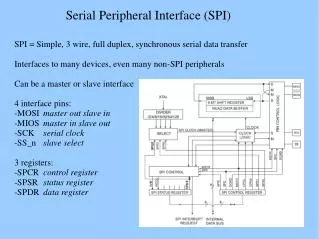
SPI SPI uses unidirectional, synchronous signals: SDO, SDI, SCLK, and SS. Only one master that initiates all transactions Every slave device requires it’s own Slave Select (SS) signal
SPI SPI uses unidirectional, synchronous signals: SDO, SDI, SCLK, and SS. Only one master that initiates all transactions Every slave device requires it’s own Slave Select (SS) signal Master-In Slave-Out (MISO) signal is typically tri-state
SPI Data is always transferred in both directions with every bus transaction Many slaves only produce data – what to write? Accelerometer, Gyro, compass, temperature, A/D converter, etc. Many slaves only consume data – what to read? Motor controller, D/A, LED driver, LCD display, etc.
SPI with multiple slaves Only one master that initiates all transactions Every slave device requires it’s own Slave Select (SS) signal Master-In Slave-Out (MISO) signal is typically tri-state
SPI data protocol… … there is none. Every SPI device can have a unique data protocol. Very flexible and powerful, but… Must read and understand the data sheet. SPI flow control… … there is none. SPI devices must implement their own checks for overflow, timeouts, etc.
Synchronous Communications SS (almost always active low) starts/defines a data frame. Eight or more clocks per data frame move data through continuous shift register.
Synchronous Communications The SPI spec allows for different clock frequencies and different clock polarities. Imagine a stream of data. Which edge should the slave use to drive the bus? Which edge should the master use to read the bus?
SPI clock phase Leading edge vs. next edge “Inside” current transaction vs. “outside”
SPI relative advantages • Transmitter and receiver use same clock; a precision clock is not needed. Period, phase and duty cycle can vary widely, provided the minimum clock period requirement is met • No address needed since SPI is point-to-point • Signals are unidirectional so three state buffers and bus turn-around circuits are not needed • Any data size can be used (not just 8 bits) • No arbitration or clock extraction is needed since the clock is included in the bus • No special transceivers are needed – SPI signals are simple logic-level signals
SPI relative disadvantages • Since the bus is point-to-point, more pins are required to interface with more devices • The SPI protocol does not include flow control, data acknowledge, or error checking, so the master has no good way to know whether data was accurately sent and received • Only one master is defined, so the bus cannot be shared So… is SPI a good choice?
QSPI As SPI became more popular, it’s bandwidth limitation (about 5MBytes) began to be recognized (particularly for mass-store devices) But, low pin-count is very desirable. QSPI: 4 data pins (everything else is the same) in 8-pin package (don’t forget Vdd and GND!)
SD cards Secure Digital cards: very small, power efficient, low-cost, popular SD/SDIO physical pins are more or less QSPI, but protocol is unique Default speed: 25MHz; High speed 50MHz Spec is free! UHS-1 and USH-2 Same pinout and form-factor as SD Single-ended I/O at up to 104MHz UHS-2 Adds more pins Adds differential signaling at lower voltages (1.8V) Adds DDR option
SPI on ZYNQ Two independent SPI controllers Can use MIO pins or EMIO (via FPGA) pins
ZYNQ’s UART FIFOs TXD and RXD path have 64-byte FIFOs
Baud Generator SCK = 166MHz / 2 n + 1 where n is defined by bits 5:3 in configuration register
Configuring the SPI controller The SPI controller is a “protected resource”, so access must be unlocked. “System Level Control Registers” control access to most on-board peripherals. Access is unlocked by writing “DF0D” to address 0xF800 0002 (this is fixed by chip designers) After unlocking, SPI system can be reset, and then it can be configured
Configuring the SPI controller #define MOD_RESET_BASEADDR 0xF8000000 void SPI_reset() { uint32_t register_value; *((uint32_t *) MOD_RESET_BASEADDR+0x8/4) = 0x0000DF0D; // unlock the SLCRs *((uint32_t *) MOD_RESET_BASEADDR + 0x0000021C/4) = 0xF; // Reset SPI0 *((uint32_t *) MOD_RESET_BASEADDR + 0x0000021C/4) = 0; // Release the reset return; }
Configuring ZYNQ’s SPI Controller Enable ModeFail generation; Set Manual Start Command to 0; Set Manual Start Enable to Auto mode; Enable Manual CS (CS is used here for SS); Set CS to 0xF to de-assert all the slave selects before the start of transfers; Set Peripheral select decode to only 1 of 3 selects; Set the Master Reference Clock Select to SPI Reference Clock (166.66666MHz) Set Baud Rate Division value to 32 to select an SPI SCLK frequency below 10MHz as required by the inertial module (see the inertial module data sheet for more information); Use SPI Mode 3 by setting the clock phase to “clock is inactive outside the word” and the polarity to quiescent high (CPOL = 1 & CPHA =1); Select SPI in the master mode.
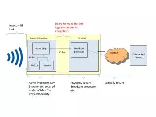
ZYNQ’s Inertial Module The Blackboard includes an LSM9DS1 inertial module from ST Microelectronics (see https://www.st.com/resource/en/datasheet/DM00103319.pdf ) • The LSM9DS1 includes: • a 3-axis accelerometer (linear acceleration) • a 3-axis gyro (angular rate of change) • a 3-axis magnetometer (magnetic field strength) The LSM9DS1 is connected to SPI0 through the EMIO interface
ZYNQ’s Inertial Module The LSM9DS1 uses two SS signals: one for ACC/Gyro, one for Mag (must drive SS signals independently)
ZYNQ’s Inertial Module The LSM9DS1 SPI interface can use an SCLK up to 10MHz All transfers are 16-bits Read: set R/W bit, send register address, then 0x00 Write: set R/W bit, send register address, then data
ZYNQ’s Inertial Module Enable the SPI Controller by writing to the ZYNQ/SPI ER register; Assert the Accelerometer/Gyro SS signal by writing “1110” to the CS bit field in the Configuration Register (or to read magnetometer data, assert it’s SS by writing 1101 to those same bits); Move data through the SPI registers by writing the R/W bit, register address, and 0x00 (16 bits total) to the transmit FIFO; Poll on Transmitter FIFO Underflow using the SPI0 SR register; Read the two data bytes from the receive data FIFO; Disable controller SPI controller (again using the ER register) De-assert the SS signal (by writing 0xF to the CS bit fields in the Configuration register.