Download
1 / 17
170 likes | 410 Views
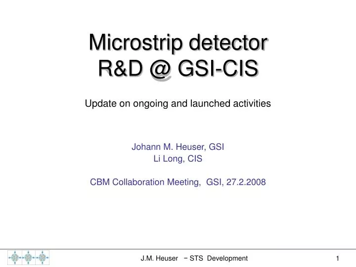
Microstrip detector R&D @ GSI-CIS. Update on ongoing and launched activities. Johann M. Heuser, GSI Li Long, CIS CBM Collaboration Meeting, GSI, 27.2.2008. I. II. n side: "vertical" strips. p side "double metal". blue: double metal connect- ions of strips I to III. III.

E N D
Microstrip detector R&D @ GSI-CIS Update on ongoing and launched activities Johann M. Heuser, GSILi Long, CIS CBM Collaboration Meeting, GSI, 27.2.2008 J.M. Heuser − STS Development
I II n side:"vertical" strips p side"double metal" blue:double metal connect-ions of strips I to III III Technical challenge • tracking station with readout electronics outside of the aperture • 2 projective coordinates,if possible in one thin silicon layer: double-sided strip detector • electrical contacts at sensor's top/bottom edge: ladder construction • no "dead" region in the corners, despite of strips oriented under a stereo angle. • high radiation tolerance: design, material • 1st R&D study GSI-CIS: "CBM01" - focus on connectivity • Double-sided detector, with double-metal connections of strips in the corner regions contact pad rows at top and bottom edge. CBM STS tracking station Detector module readout direction J.M. Heuser − STS Development
Microstrip detector prototype CBM01, 8/2007 Test sensors 4" wafer, 285 µm Si Double-sided, single-metal, 256256 strips, orthogonal, 50(80) µm pitch, size: 1414 (22 22)mm2 Main sensor Double-sided, double-metal, 1024 strips per side, 50 µm pitch, 15º stereo angle, full-area sensitive, contacts at top + bottom edge, size: 5656 mm2 J.M. Heuser − STS Development
1/C2 [pF-2] I [µA] I [µA] U [V] U [V] U[V] Characterization at CIS IV and CV behaviour of CBM01B1, CBM01B2, CBM02 (Mr. John et al.) reported at CBM Meeting September 2007 J.M. Heuser − STS Development
Find application in various activities of beginning detector module R&D Only available CBM-specific microstrip detectors GSI: Test board (CBM01B2, preparation, report A. Lymanets) Test beam tracking module (planned) KINR Kiev: Pre-prototype module & CBM01B1 detector tests (electrical, diode laser, radioactive source) (report V. Pugatch) Kharkov: Test board with microcable fanout structure (planned) Cracow: n-XYTER-SUCIMA board with CBM01B2 (planned) + many new ideas ooo ooo ooo J.M. Heuser − STS Development
Towards 2nd design iteration • CIS activity in frame of german BMWI project INNOWAT -“SPID“: • Test wafer to explore primarilyradiation tolerance • Bias method: punch-through, poly-silicon • Breakdown voltage: charge, micro discharge • Insulation technology: p-spray , p-stop, field plate J.M. Heuser − STS Development
Second manufacture run ("technology wafer") L. Long and R. Rolf, CIS Full detectors 7 pixel detectors; 18 strip detectors. Test structures: 3 Pad diodes, 4 Gate diodes, 6 PDTF, 2 SIMS, 2 SDM. Process status 2/2008: First active implant finished. J.M. Heuser − STS Development
Simulation of electrical properties Technology simulation:resistance for p front 66 kOhm/cm resistance for n back 44 kOhm/cm Layout calculation: coupling capacitance front 21 pF/cm coupling capacitance back 15 pF/cm resistance for front metal 25 Ohm/cm resistance for back metal 16 Ohm/cm resistance for cross connection 28 Ohm/cm Electrical field: ohmic side junction side J.M. Heuser − STS Development
Technology variations in detail (I) Wafers with different processing J.M. Heuser − STS Development
Technology variations in detail (II) Detectors and test structures on the wafers J.M. Heuser − STS Development
Technology variations in detail (III) Detectors and test structures on the wafers J.M. Heuser − STS Development
Polysilicon bias structures New at CIS. • The designed poly resistors has 230 squares, the sheet resist should be 4.3k/Sq by 1M and 6.5k /Sq by 1.5M. • For Test wafer we need only two masks. • Flow card for poly-resist test: Processing steps: LTO deposition Poly-Silicon deposition Oxidation. Implantation Boron variations Removing of oxid Photolithography and patterning Aluminium 1µm Photolithography and patterning J.M. Heuser − STS Development
Interstrip capacitance of the CBM01 detector L. Long, CiS Erfurt, 21.02.2008 Requirement of n-XYTER front end to the inter strip capacitance of the CBM01 detector: It seems that Ctotal (Ccable + Cint_detector+ Cin_n-XYTER) ~< 30pF. Cint = capacitance of one strip against the two neighbour strips connected together, at frequency 10kHz and 100kHz. Rint = resistance of one strip against the two neighbour strips connected together. Both of them are tested at full depletion condition. Comparison between CBM01 and ALICE microstrip detector: J.M. Heuser − STS Development
Electrical simulations, r/o cable (L. Long, CIS) Simple model: Five strip lines are considered. Middle strip 1V, all other strips 0V. Inter-strip capacitance: 2 × 0.4 = 0.8 pF/cm. noise load for FE electronics. J.M. Heuser − STS Development
Signal-to-noise in a detector system Simple exercise: (J. Heuser) Cable: ~0.8 pF/cm Sensor: typically 1.5 pF/cm strip n-XYTER: ENC 26.9 e/pF + 200 e (fast channel) 12.7 e/pF + 233 e (slow channel) Signal in 280 µm Si: 80 e/µm × 280 µm = 22 400 e Let‘s assume an average detector module: 6cm strip + 30 cm cable: Cinterstrip = 35 pF→n-XYTER will see ENC @ 35 pF = 1100 e S/N (22 400 e) = 20S/N (11 200 e, charge shared by 2 strips) = 10 on the edge ? J.M. Heuser − STS Development
Summary/Outlook • Cooperation GSI-CiS on microstrip detector development and production for CBM is very effective. • First detector prototypes CBM01 have been fabricated in 2007 after an intensive, innovative preparation phase in 2006. • Extremely useful now for STS prototyping. Many teams depend on these detectors for the R&D tasks. • Currently under production: "Technology wafer" for improved next version of the CBM microstrip detectors. Prime target: Radiation hardness. • Next full detector design: Will probably take some time, first need evaluation from 1st wafer and from "technology" wafer, CBM needs to specify its further requirements. • Next project with CiS involvement: Single-sided strip detectors? J.M. Heuser − STS Development
ALICE & ATLAS industry awards to CiS CIS has been subcontractor of Canberra for the ALICE microstrip detectors. Cern made the specification, Canberra made the design, CiS made the whole processing. In 2006, the ALICE detectors from CiS received an award from CERN (through CANBERRA). J.M. Heuser − STS Development