Download
1 / 29
290 likes | 395 Views
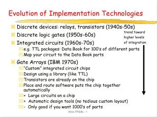
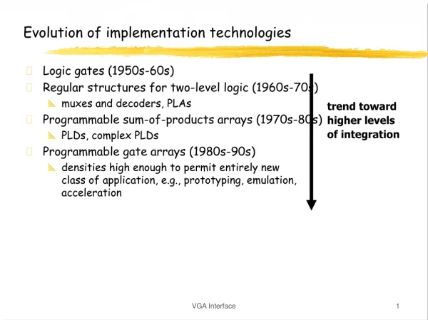
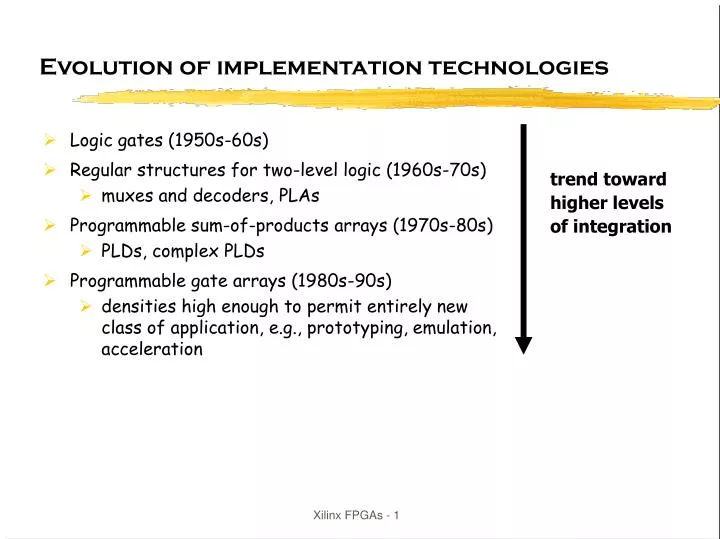
Evolution of implementation technologies. Logic gates (1950s-60s) Regular structures for two-level logic (1960s-70s) muxes and decoders, PLAs Programmable sum-of-products arrays (1970s-80s) PLDs, complex PLDs Programmable gate arrays (1980s-90s)

E N D
Evolution of implementation technologies • Logic gates (1950s-60s) • Regular structures for two-level logic (1960s-70s) • muxes and decoders, PLAs • Programmable sum-of-products arrays (1970s-80s) • PLDs, complex PLDs • Programmable gate arrays (1980s-90s) • densities high enough to permit entirely newclass of application, e.g., prototyping, emulation,acceleration trend toward higher levels of integration Xilinx FPGAs - 1
Gate Array Technology (IBM - 1970s) • Simple logic gates • combine transistors toimplement combinationaland sequential logic • Interconnect • wires to connect inputs andoutputs to logic blocks • I/O blocks • special blocks at peripheryfor external connections • Add wires to make connections • done when chip is fabbed • “mask-programmable” • construct any circuit Xilinx FPGAs - 2
Field-Programmable Gate Arrays • Logic blocks • to implement combinationaland sequential logic • Interconnect • wires to connect inputs andoutputs to logic blocks • I/O blocks • special logic blocks at peripheryof device for external connections • Key questions: • how to make logic blocks programmable? • how to connect the wires? • after the chip has been fabbed Xilinx FPGAs - 3
Enabling Technology • Cheap/fast fuse connections • small area (can fit lots of them) • low resistance wires (fast even if in multiple segments) • very high resistance when not connected • small capacitance (wires can be longer) • Pass transistors (switches) • used to connect wires • bi-directional • Multiplexors • used to connect one of a set of possible sources to input • can be used to implement logic functions Xilinx FPGAs - 4
Programming Technologies • Fuse and anti-fuse • fuse makes or breaks link between two wires • typical connections are 50-300 ohm • one-time programmable • Flash • High density • Process issues • RAM-based • memory bit controls a switch that connects/disconnects two wires • typical connections are .5K-1K ohm • can be programmed and re-programmed easily (tested at factory) Xilinx FPGAs - 5
Tradeoffs in FPGAs • Logic block - how are functions implemented: fixed functions (manipulate inputs) or programmable? • support complex functions, need fewer blocks, but they are bigger so less of them on chip • support simple functions, need more blocks, but they are smaller so more of them on chip • Interconnect • how are logic blocks arranged? • how many wires will be needed between them? • are wires evenly distributed across chip? • programmability slows wires down – are some wires specialized to long distances? • how many inputs/outputs must be routed to/from each logic block? • what utilization are we willing to accept? 50%? 20%? 90%? Xilinx FPGAs - 6
Xilinx Programmable Gate Arrays • CLB - Configurable Logic Block • 5-input, 1 output function • or 2 4-input, 1 output functions • optional register on outputs • Built-in fast carry logic • Can be used as memory • Three types of routing • direct • general-purpose • long lines of various lengths • RAM-programmable • can be reconfigured Xilinx FPGAs - 7
The Virtex CLB Xilinx FPGAs - 9
Details of One Virtex Slice Xilinx FPGAs - 10
Implements any Two 4-input Functions 4-input function 3-input function; registered Xilinx FPGAs - 11
Implements any 5-input Function 5-input function Xilinx FPGAs - 12
Implement Some Larger Functions e.g. 9-input parity Xilinx FPGAs - 13
Two Slices: Any 6-input Function from other slice 6-input function Xilinx FPGAs - 14
Two Slices: Implement some larger functions e.g. 19-input parity from other slice Xilinx FPGAs - 15
Fast Carry Chain: Add two bits per slice Carry(a,b,cin) Sum(a,b,cin) a b cin Xilinx FPGAs - 16
Lookup Tables used as memory (16 x 2)[ Distributed Memory ] Xilinx FPGAs - 17
Lookup Tables used as memory (32 x 1) Xilinx FPGAs - 18
Block RAM Xilinx FPGAs - 19
Virtex Routing Xilinx FPGAs - 20
Virtex Routing Xilinx FPGAs - 21
Non-Local Routing • Hex wires • Extend 6 CLBs in one direction • Connections at 3 and 6 CLBs • “Express busses” • Take advantage of many metal layers • Long wires • Extend the length/height of the chip • Global signals • e.g. clk, reset • Tri-state busses • Extend across the chip • Use for datapath bit-slice Xilinx FPGAs - 22
Using the DLL to De-Skew the Clock Xilinx FPGAs - 23
Virtex IOB Xilinx FPGAs - 24
Computer-aided Design • Can't design FPGAs by hand • way too much logic to manage, hard to make changes • Hardware description languages • specify functionality of logic at a high level • Validation - high-level simulation to catch specification errors • verify pin-outs and connections to other system components • low-level to verify mapping and check performance • Logic synthesis • process of compiling HDL program into logic gates and flip-flops • Technology mapping • map the logic onto elements available in the implementation technology (LUTs for Xilinx FPGAs) Xilinx FPGAs - 25
CAD Tool Path (cont’d) • Placement and routing • assign logic blocks to functions • make wiring connections • Timing analysis - verify paths • determine delays as routed • look at critical paths and ways to improve • Partitioning and constraining • if design does not fit or is unroutable as placed split into multiple chips • if design it too slow prioritize critical paths, fix placement of cells, etc. • few tools to help with these tasks exist today • Generate programming files - bits to be loaded into chip for configuration Xilinx FPGAs - 26
Xilinx CAD Tools • Verilog (or VHDL) use to specify logic at a high-level • combine with schematics, library components • Synplicity • compiles Verilog to logic • maps logic to the FPGA cells • optimizes logic • Xilinx APR - automatic place and route (simulated annealing) • provides controllability through constraints • handles global signals • Xilinx Xdelay - measure delay properties of mapping and aid in iteration • Xilinx XACT - design editor to view final mapping results Xilinx FPGAs - 27
Applications of FPGAs • Implementation of random logic • easier changes at system-level (one device is modified) • can eliminate need for full-custom chips • Prototyping • ensemble of gate arrays used to emulate a circuit to be manufactured • get more/better/faster debugging done than possible with simulation • Reconfigurable hardware • one hardware block used to implement more than one function • functions must be mutually-exclusive in time • can greatly reduce cost while enhancing flexibility • RAM-based only option • Special-purpose computation engines • hardware dedicated to solving one problem (or class of problems) • accelerators attached to general-purpose computers Xilinx FPGAs - 28